

Motorola ULN2068B Datasheet
Device
Operating
Temperature Range
Package
SEMICONDUCTOR
TECHNICAL DATA
QUAD 1.5 A
DARLINGTON SWITCH
ORDERING INFORMATION*
ULN2068B TA = 0 to +70°C Plastic DIP
B SUFFIX
PLASTIC PACKAGE
CASE 648C
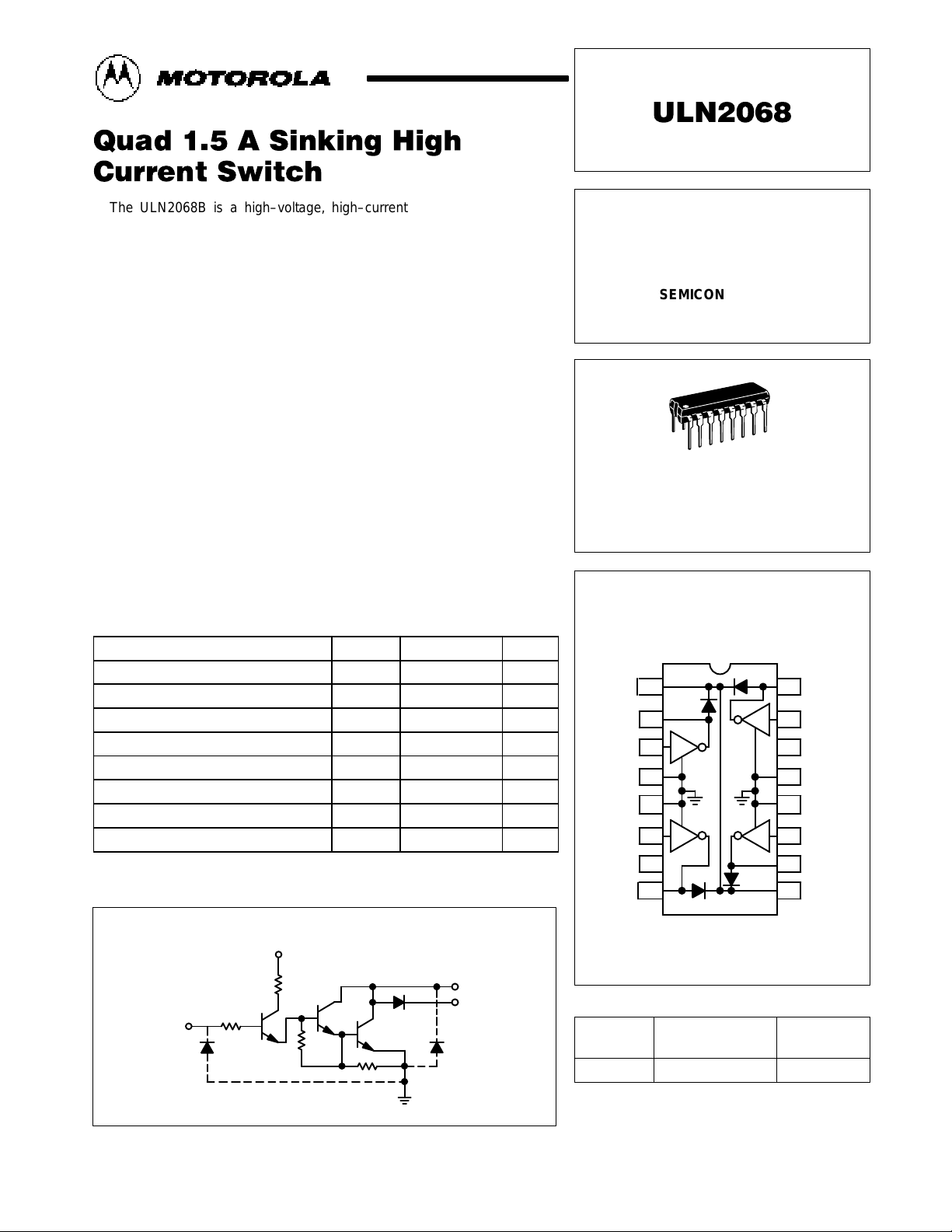
PIN CONNECTIONS
Order this document by ULN2068/D
K
C
B
Gnd
Gnd
V
S
B
C
C
NC
B
Gnd
Gnd
B
C
K 1
2
3
4
5
6
7
8
16
15
14
13
12
11
10
9
*Other options of this ULN2060/2070 series are available
*for volume applications. Contact your local Motorola Sales
*Representative.
1
MOTOROLA ANALOG IC DEVICE DATA
The ULN2068B is a high–voltage, high–current quad Darlington switch
array designed for high current loads, both resistive and reactive, up to 300 W .
It is intended for interfacing between low level (TTL, DTL, LS and 5.0 V
CMOS) logic families and peripheral loads such as relays, solenoids, dc and
stepping motors, multiplexer LED and incandescent displays, heaters, or other
high voltage, high current loads.
The Motorola ULN2068B is specified with minimum guaranteed breakdown
of 50 V and is 100% tested for safe area using an inductive load. It includes
integral transient suppression diodes. Use of a predriver stage reduces input
current while still allowing the device to switch 1.5 Amps.
It is supplied in an improved 16–Pin plastic DIP package with heat sink
contact tabs (Pins 4, 5, 12 a nd 13). A c opper a lloy lead frame allows maximum
power dissipation using standard cooling techniques. The use of the contact
tab lead frame facilitates attachment of a DIP heat sink while permitting the
use of standard layout and mounting practices.
• TTL, DTL, LS, CMOS Compatible Inputs
• 1.5 A Maximum Output Current
• Low Input Current
• Internal Freewheeling Clamp Diodes
• 100% Inductive Load Tested
• Heat Tab Copper Alloy Lead Frame for Increased Dissipation
MAXIMUM RATINGS (T
A
= 25°C and ratings apply to any one device in the
package, unless otherwise noted)
Rating
Symbol Value Unit
Output Voltage V
O
50 V
Input Voltage (Note 1) V
I
15 V
Supply Voltage V
S
10 V
Collector Current (Note 2) I
C
1.75 A
Input Current (Note 3) I
I
25 mA
Operating Ambient Temperature Range T
A
0 to +70 °C
Storage Temperature Range T
stg
–55 to +150 °C
Junction Temperature T
J
150 °C
NOTES: 1.Input voltage referenced to ground.
2.Allowable output conditions shown in Figures 11 and 12.
3.May be limited by max input voltage.
Partial Schematic
C
3.0 k
7.2 k
R
S
0.9 k
B
R
in
2.5 k
V
S
K
Motorola, Inc. 1995
ULN2068
2
MOTOROLA ANALOG IC DEVICE DATA
ELECTRICAL CHARACTERISTICS
(TA = 25°C unless otherwise noted.)
Characteristic
Symbol Min Typ Max Unit
Output Leakage Current (Figure 1)
(VCE = 50 V)
(VCE = 50 V, TA = 70°C)
I
CEX
–
–
–
–
100
500
µA
Collector–Emitter Saturation Voltage (Figure 2)
(IC = 500 mA
(IC = 750 mA
(IC = 1.0 A
(IC = 1.25 A
Vin = 2.4 V)
V
CE(sat)
–
–
–
–
–
–
–
–
1.13
1.25
1.40
1.60
V
Input Current – On Condition (Figure 4)
(VI = 2.4 V)
(VI = 3.75 V)
I
I(on)
–
–
–
–
0.25
1.0
mA
Input Voltage – On Condition (Figure 5)
(VCE = 2.0 V, IC = 1.5 A)
V
I(on)
– – 2.4
V
Inductive Load Test (Figure 3)
(VS = 5.5 V, VCC = 24.5 V,
tPW =
4.0 ms)
∆V
out
– – 100
mV
Supply Current (Figure 8)
(IC = 500 mA, Vin = 2.4 V, VS = 5.5 V)
I
S
– – 6.0
mA
Turn–On Delay Time
(50% EI to 50% EO)
t
PHL
– – 1.0
µs
Turn–Off Delay Time
(50% EI to 50% EO)
t
PLH
– – 4.0
µs
Clamp Diode Leakage Current (Figure 6)
(VR = 50 V)
(VR = 50 V, TA = 70°C)
I
R
–
–
–
–
50
100
µA
Clamp Diode Forward Voltage (Figure 7)
(IF = 1.0 A)
(IF = 1.5 A)
V
F
–
–
–
–
1.75
2.0
V
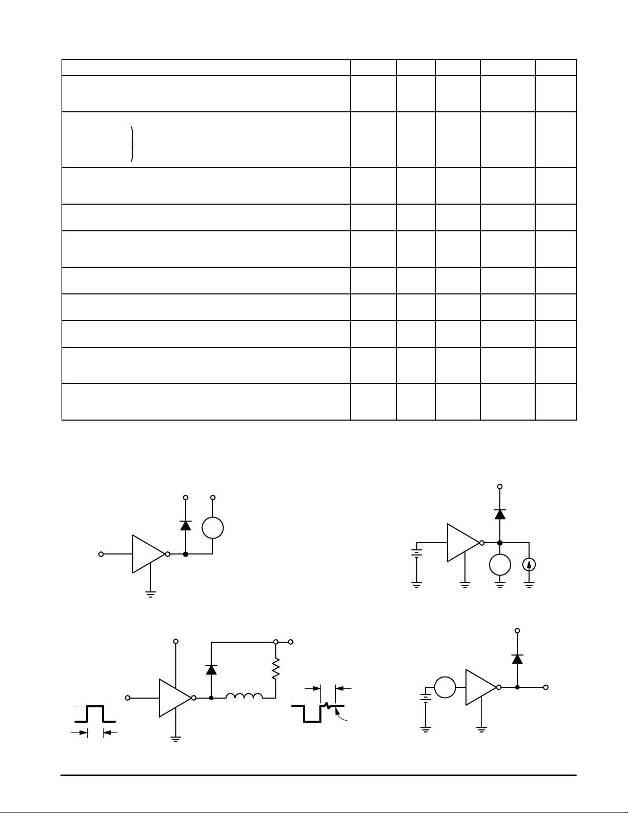
TEST FIGURES
9
70 MH
20
Ω
V
CC
V
S
t
PW
I
C
I
in
∆V
out
= V
out1
– V
out2
V
CE
Open
µ
A
Open
I
CEX
0
DUT
14 ms
5.0
V
V
in
Open
V
CE
DUT
V
in
DUT
DUT
mA
Open
V
in
Open
V
out
1
V
out
2
Figure 1. Figure 2.
Figure 3. Figure 4.
 Loading...