

Motorola UC3843AN, UC3843AD, UC3842AN Datasheet
The UC3842A, UC3843A series of high performance fixed frequency
current mode controllers are specifically designed for off–line and dc–to–dc
converter applications offering the designer a cost effective solution with
minimal external components. These integrated circuits feature a trimmed
oscillator for precise duty cycle control, a temperature compensated
reference, high gain error amplifier, current sensing comparator, and a high
current totem pole output ideally suited for driving a power MOSFET.
Also included are protective features consisting of input and reference
undervoltage lockouts each with hysteresis, cycle–by–cycle current limiting,
programmable output deadtime, and a latch for single pulse metering.
These devices are available in an 8–pin dual–in–line plastic package as
well as the 14–pin plastic surface mount (SO–14). The SO–14 package has
separate power and ground pins for the totem pole output stage.
The UCX842A has UYLO thresholds of 16 V (on) and 10 V (off), ideally
suited for off–line converters. The UCX843A is tailored for lower voltage
applications having UVLO thresholds of 8.5 V (on) and 7.6 V (off).
• Trimmed Oscillator Discharge Current for Precise Duty Cycle Control
• Current Mode Operation to 500 kHz
• Automatic Feed Forward Compensation
• Latching PWM for Cycle–By–Cycle Current Limiting
• Internally Trimmed Reference with Undervoltage Lockout
• High Current Totem Pole Output
• Undervoltage Lockout with Hysteresis
• Low Startup and Operating Current
• Direct Interface with Motorola SENSEFET Products
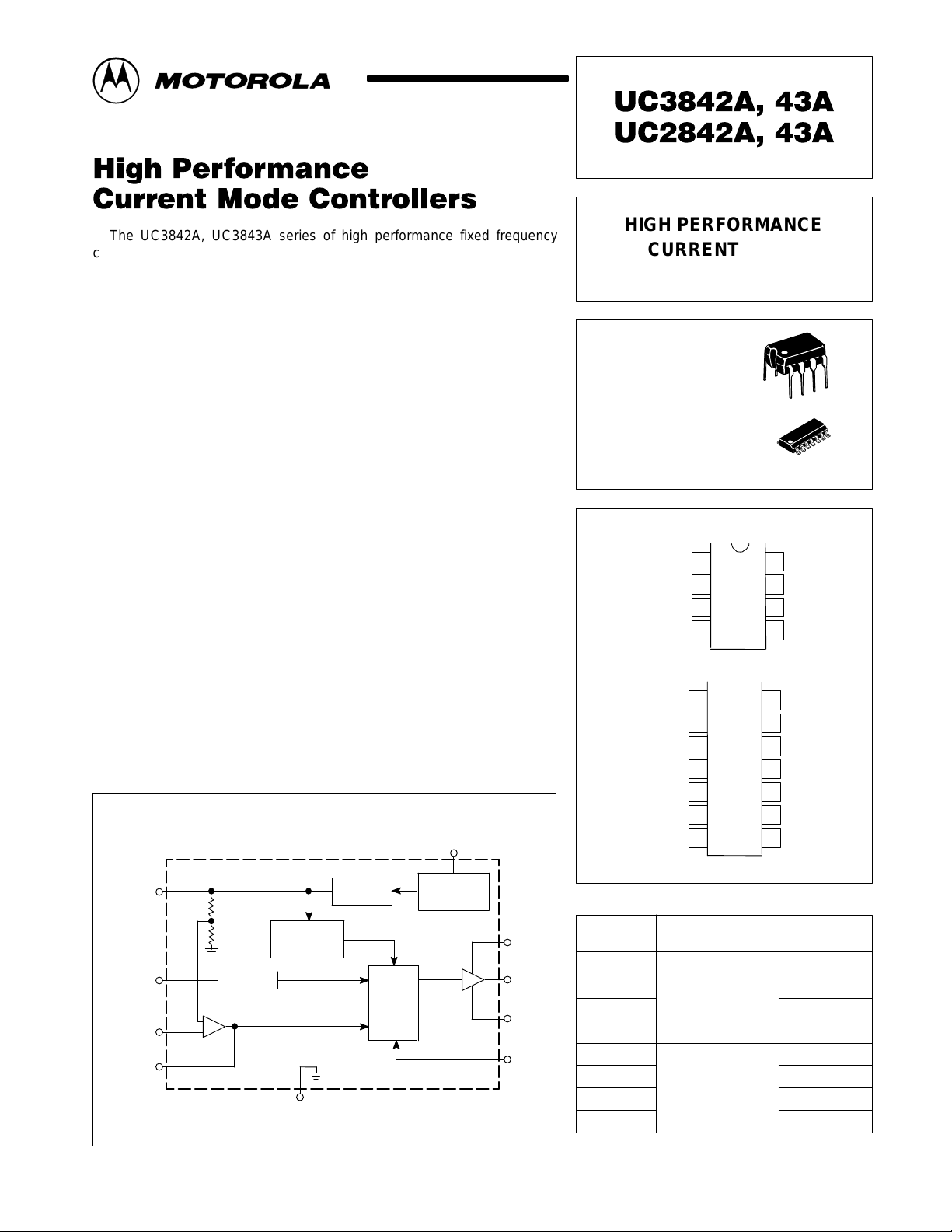
Simplified Block Diagram
V
7(12)
CC
V
ref
8(14)
RTC
4(7)
Voltage
Feedback
Input
2(3)
Output
Compensation
1(1)
5.0V
R
R
T
Oscillator
+
–
Error
Amplifier
Pin numbers in parenthesis are for the D suffix SO–14 package.
Undervoltage
Lockout
Gnd 5(9)
Reference
V
ref
Latching
PWM
V
CC
Undervoltage
Lockout
V
C
7(11)
Output
6(10)
Power
Ground
5(8)
3(5)
Current
Sense
Input
Order this document by UC3842A/D
HIGH PERFORMANCE
CURRENT MODE
CONTROLLERS
N SUFFIX
PLASTIC PACKAGE
CASE 626
D SUFFIX
PLASTIC PACKAGE
CASE 751A
(SO–14)
Compensation
Voltage Feedback
Current Sense
RT/C
Compensation
Voltage Feedback
Current Sense
RT/C
ORDERING INFORMATION
Device
UC3842AD
UC3843AD
UC3842AN
UC3843AN
UC2842AD
UC2843AD
UC2842AN
UC2843AN
Temperature Range
TA = – 25° to +85°C
PIN CONNECTIONS
1
2
3
45
T
1
2
NC
3
4
NC
5
6
NC
7
T
Operating
TA = 0° to +70°C
8
(T op View)
(T op V iew)
1
14
1
8
V
ref
7
V
CC
6
Output
Gnd
14
V
ref
13
NC
12
V
CC
11
V
C
10
Output
9
Gnd
Power Ground
8
Package
SO–14
SO–14
Plastic
Plastic
SO–14
SO–14
Plastic
Plastic
MOTOROLA ANALOG IC DEVICE DATA
Motorola, Inc. 1996 Rev 1
1
UC3842A, 43A UC2842A, 43A
MAXIMUM RATINGS
Rating Symbol Value Unit
Total Power Supply and Zener Current (ICC + IZ) 30 mA
Output Current, Source or Sink (Note 1) I
O
Output Energy (Capacitive Load per Cycle) W 5.0 µJ
Current Sense and Voltage Feedback Inputs V
Error Amp Output Sink Current I
in
O
Power Dissipation and Thermal Characteristics
D Suffix, Plastic Package
Maximum Power Dissipation @ TA = 25°C
Thermal Resistance, Junction–to–Air
N Suffix, Plastic Package
Maximum Power Dissipation @ TA = 25°C
Thermal Resistance, Junction–to–Air
Operating Junction Temperature T
Operating Ambient Temperature
UC3842A, UC3843A
P
D
R
θJA
P
D
R
θJA
J
T
A
UC2842A, UC2843A
Storage Temperature Range T
stg
1.0 A
– 0.3 to + 5.5 V
10 mA
862
145
1.25
100
+ 150 °C
0 to + 70
– 25 to + 85
– 65 to + 150 °C
mW
°C/W
W
°C/W
°C
ELECTRICAL CHARACTERISTICS (V
= 15 V, [Note 2], RT = 10 k, CT = 3.3 nF, TA = T
CC
low
to T
high
[Note 3],
unless otherwise noted.)
UC284XA UC384XA
Characteristics Symbol Min Typ Max Min Typ Max Unit
REFERENCE SECTION
Reference Output Voltage (IO = 1.0 mA, TJ = 25°C) V
Line Regulation (VCC = 12 V to 25 V) Reg
Load Regulation (IO = 1.0 mA to 20 mA) Reg
T emperature Stability T
Total Output V ariation over Line, Load, Temperature V
Output Noise Voltage (f = 10 Hz to 10 kHz, TJ = 25°C) V
ref
line
load
S
ref
n
4.95 5.0 5.05 4.9 5.0 5.1 V
– 2.0 20 – 2.0 20 mV
– 3.0 25 – 3.0 25 mV
– 0.2 – – 0.2 – mV/°C
4.9 – 5.1 4.82 – 5.18 V
– 50 – – 50 – µV
Long Term Stability (TA = 125°C for 1000 Hours) S – 5.0 – – 5.0 – mV
Output Short Circuit Current I
SC
– 30 – 85 – 180 – 30 – 85 – 180 mA
OSCILLATOR SECTION
Frequency
TJ = 25°C
TA = T
low
to T
high
Frequency Change with Voltage (VCC = 12 V to 25 V) ∆f
Frequency Change with Temperature
TA = T
low
to T
high
Oscillator Voltage Swing (Peak–to–Peak) V
Discharge Current (V
TJ = 25°C
TA = T
NOTES: 1. Maximum Package power dissipation limits must be observed.
to T
low
2.Adjust VCC above the Startup threshold before setting to 15 V.
3.Low duty cycle pulse techniques are used during test to maintain junction temperature as close to ambient as possible
T
= –20°C for UC3842A, UC3843A T
low
T
= –25°C for UC2842A, UC2843A T
low
high
osc
= 2.0 V)
f
osc
47
46
osc/∆V
∆f
osc/∆T
I
dischg
osc
– 0.2 1.0 – 0.2 1.0 %
– 5.0 – – 5.0 – %
– 1.6 – – 1.6 – V
7.5
7.2
= +70°C for UC3842A, UC3843A
high
= +85°C for UC2842A, UC2843A
high
52
8.4
–
60
9.3
57
–
9.5
47
46
7.5
7.2
52
8.4
–
60
9.3
57
–
9.5
kHz
mA
2
MOTOROLA ANALOG IC DEVICE DATA
UC3842A, 43A UC2842A, 43A
ELECTRICAL CHARACTERISTICS (V
= 15 V, [Note 2], RT = 10 k, CT = 3.3 nF, TA = T
CC
low
to T
high
[Note 3],
unless otherwise noted.)
UC284XA UC384XA
Characteristics Symbol Min Typ Max Min Typ Max Unit
ERROR AMPLIFIER SECTION
Voltage Feedback Input (VO = 2.5 V) V
Input Bias Current (VFB = 2.7 V) I
Open Loop Voltage Gain (VO = 2.0 V to 4.0 V) A
FB
IB
VOL
2.45 2.5 2.55 2.42 2.5 2.58 V
– –0.1 –1.0 – –0.1 –2.0 µA
65 90 – 65 90 – dB
Unity Gain Bandwidth (TJ = 25°C) BW 0.7 1.0 – 0.7 1.0 – MHz
Power Supply Rejection Ratio (VCC = 12 V to 25 V) PSRR 60 70 – 60 70 – dB
Output Current
Sink (VO = 1.1 V, VFB = 2.7 V)
Source (VO = 5.0 V, VFB = 2.3 V)
I
Sink
I
Source
2.0
–0.512–1.0
–
–
2.0
–0.512–1.0
–
–
Output Voltage Swing
High State (RL = 15 k to ground, VFB = 2.3 V)
Low State (RL = 15 k to V
, VFB = 2.7 V)
ref
V
OH
V
OL
5.0
–
6.2
0.8
1.1
–
5.0
–
0.8
6.2
–
1.1
CURRENT SENSE SECTION
Current Sense Input Voltage Gain (Notes 4 & 5) A
Maximum Current Sense Input Threshold (Note 4) V
Power Supply Rejection Ratio
PSRR
VCC = 12 to 25 V (Note 4)
Input Bias Current I
Propagation Delay (Current Sense Input to Output) t
PLH(in/out)
V
th
IB
2.85 3.0 3.15 2.85 3.0 3.15 V/V
0.9 1.0 1.1 0.9 1.0 1.1 V
– 70 – – 70 –
– –2.0 –10 – –2.0 –10 µA
– 150 300 – 150 300 ns
OUTPUT SECTION
Output Voltage
Low State (I
Low State (I
High State (I
High State (I
Output Voltage with UVLO Activated
VCC = 6.0 V, I
Output Voltage Rise T ime (CL = 1.0 nF, TJ = 25°C) t
Output Voltage Fall T ime (CL = 1.0 nF, TJ = 25°C) t
Sink
Sink
Sink
Sink
Sink
= 20 mA)
= 200 mA)
= 20 mA)
= 200 mA)
= 1.0 mA
V
OL
V
OH
V
OL(UVLO)
r
f
–
–
13
12
0.1
1.6
13.5
13.4
0.4
2.2
–
–
–
–
13
12
0.1
1.6
13.5
13.4
0.4
2.2
–
–
– 0.1 1.1 – 0.1 1.1
– 50 150 – 50 150 ns
– 50 150 – 50 150 ns
UNDERVOLTAGE LOCKOUT SECTION
Startup Threshold
UCX842A
UCX843A
Minimum Operating Voltage After Turn–On
UCX842A
UCX843A
V
th
V
CC(min)
15
7.8
9.0
7.0
16
8.4
10
7.6
17
9.0
11
8.2
14.5
7.8
8.5
7.0
16
8.4
10
7.6
17.5
9.0
11.5
8.2
PWM SECTION
Duty Cycle
Maximum
Minimum
DC
DC
max
min
94
–
–
96
–
0
94
–
–
96
–
0
TOTAL DEVICE
Power Supply Current (Note 2)
Startup:
(VCC = 6.5 V for UCX843A,
(VCC = 14 V for UCX842A) Operating
Power Supply Zener Voltage (ICC = 25 mA) V
NOTES: 2. Adjust VCC above the Startup threshold before setting to 15 V.
3.Low duty cycle pulse techniques are used during test to maintain junction temperature as close to ambient as possible
T
= –20°C for UC3842A, UC3843A T
low
T
= –25°C for UC2842A, UC2843A T
low
4.This parameter is measured at the latch trip point with VFB = 0 V.
5.Comparator gain is defined as: A
∆V Output Compensation
V
∆V Current Sense Input
I
CC
–
–
Z
= +70°C for UC3842A, UC3843A
high
= +85°C for UC2842A, UC2843A
high
30 36 – 30 36 – V
0.5
12
1.0
17
–
–
0.5
12
1.0
17
mA
V
dB
V
V
V
V
%
mA
MOTOROLA ANALOG IC DEVICE DATA
3
UC3842A, 43A UC2842A, 43A
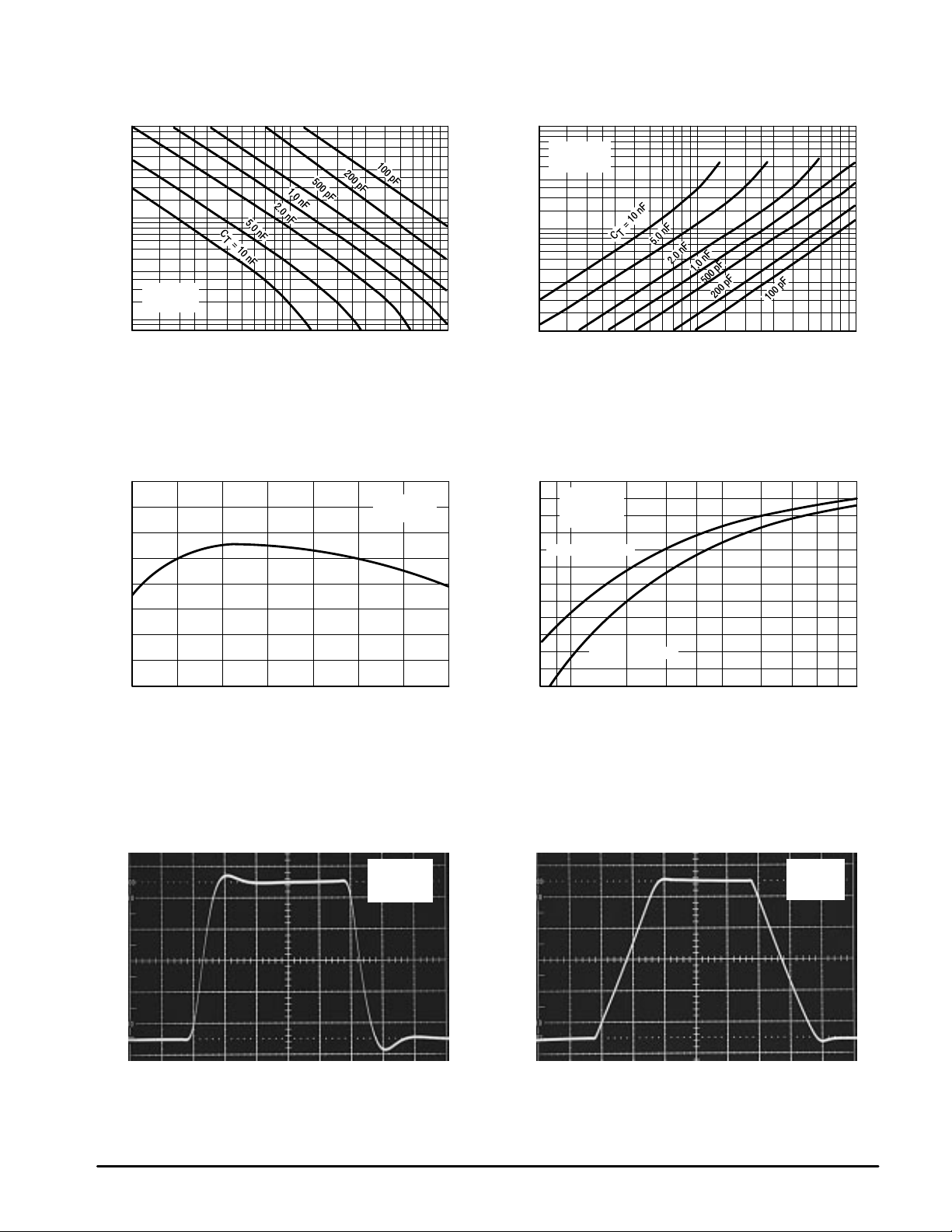
Figure 1. Timing Resistor versus
Oscillator Frequency
80
50
Ω
20
8.0
5.0
, TIMING RESISTOR (k )
VCC = 15 V
2.0
T
R
0.8
10 k 20 k 50 k 100 k 200 k 500 k 1.0 M
TA = 25
°
C
f
, OSCILLAT OR FREQUENCY (Hz)
OSC
Figure 3. Oscillator Discharge Current
versus T emperature
9.0
VCC = 15 V
V
= 2.0 V
8.5
OSC
Figure 2. Output Deadtime versus
Oscillator Frequency
100
VCC = 15 V
50
20
10
5.0
2.0
% DT, PERCENT OUTPUT DEADTIME
1.0
10 k 20 k 50 k 100 k 200 k 500 k 1.0 M
TA = 25
°
C
f
, OSCILLAT OR FREQUENCY (Hz)
OSC
Figure 4. Maximum Output Duty Cycle
versus Timing Resistor
100
VCC = 15 V
CT = 3.3 nF
90
80
I
TA = 25
dischg
°
C
= 7.2 mA
8.0
, DISCHARGE CURRENT (mA)
7.5
dischg
I
7.0
–55 –25 0 25 50 75 100 125
TA, AMBIENT TEMPERATURE (
°
C)
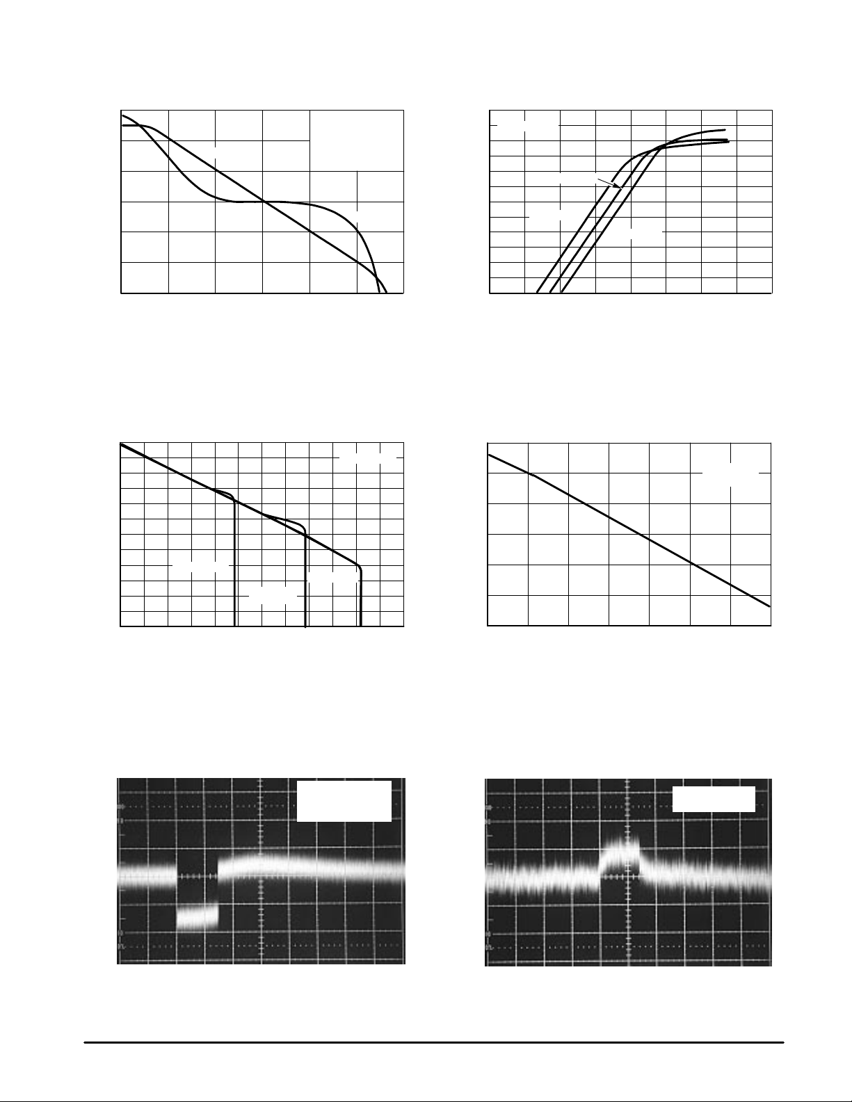
Figure 5. Error Amp Small Signal
Transient Response
VCC = 15 V
2.55 V
2.5 V
AV = –1.0
TA = 25
70
60
50
, MAXIMUM OUTPUT DUTY CYCLE (%)
max
D
40
800 1.0 k 2.0 k 3.0 k 4.0 k 6.0 k 8.0 k
I
= 9.5 mA
dischg
RT, TIMING RESISTOR (Ω)
Figure 6. Error Amp Large Signal
Transient Response
VCC = 15 V
°
C
20 mV/DIV
3.0 V
2.5 V
AV = –1.0
°
TA = 25
C
200 mV/DIV
2.45 V
4
0.5 µs/DIV
2.0 V
0.1 µs/DIV
MOTOROLA ANALOG IC DEVICE DATA
UC3842A, 43A UC2842A, 43A
Figure 7. Error Amp Open Loop Gain and
Phase versus Frequency
100
80
60
40
20
, OPEN LOOP VOL TAGE GAIN (dB)
0
VOL
A
–20
100 1.0 k 10 k 100 k 1.0 M
Gain
f, FREQUENCY (Hz)
Figure 9. Reference V oltage Change
versus Source Current
0
–4.0
–8.0
VCC = 15 V
VO = 2.0 V to 4.0 V
RL = 100 K
°
C
TA = 25
Phase
VCC = 15 V
0
30
60
90
120
150
180
10 M10
1.2
1.0
0.8
0.6
0.4
, EXCESS PHASE (DEGREES)
0.2
φ
, CURRENT SENSE INPUT THRESHOLD (V)
th
0
V
0
110
90
Figure 8. Current Sense Input Threshold
versus Error Amp Output Voltage
VCC = 15 V
TA = 25°C
TA = 125°C
TA = –55°C
2.0 4.0 6.0 8.0
VO, ERROR AMP OUTPUT VOLTAGE (V)
Figure 10. Reference Short Circuit Current
versus T emperature
VCC = 15 V
≤
0.1
RL
Ω
–12
–16
, REFERENCE VOLTAGE CHANGE (mV)
–20
ref
V
∆
–24
0 20 40 60 80 100 120
TA = 125°C
TA = 25°C
I
, REFERENCE SOURCE CURRENT (mA)
ref
TA = 55°C
Figure 11. Reference Load Regulation
VCC = 15 V
IO = 1.0 mA to 20 mA
°
C
TA = 25
70
, REFERENCE SHORT CIRCUIT CURRENT (mA)
50
SC
I
–55 –25 0 25 50 75 100 125
°
TA, AMBIENT TEMPERATURE (
C)
Figure 12. Reference Line Regulation
VCC = 12 V to 25 V
°
C
TA = 25
, OUTPUT VOLTAGE CHANGE (2.0 mV/DIV)
O
V
∆
2.0 ms/DIV
MOTOROLA ANALOG IC DEVICE DATA
, OUTPUT VOLTAGE CHANGE (2.0 mV/DIV)
O
V
∆
2.0 ms/DIV
5
 Loading...