

Motorola TCF6000D, TCF6000 Datasheet
Order this document by TCF6000/D
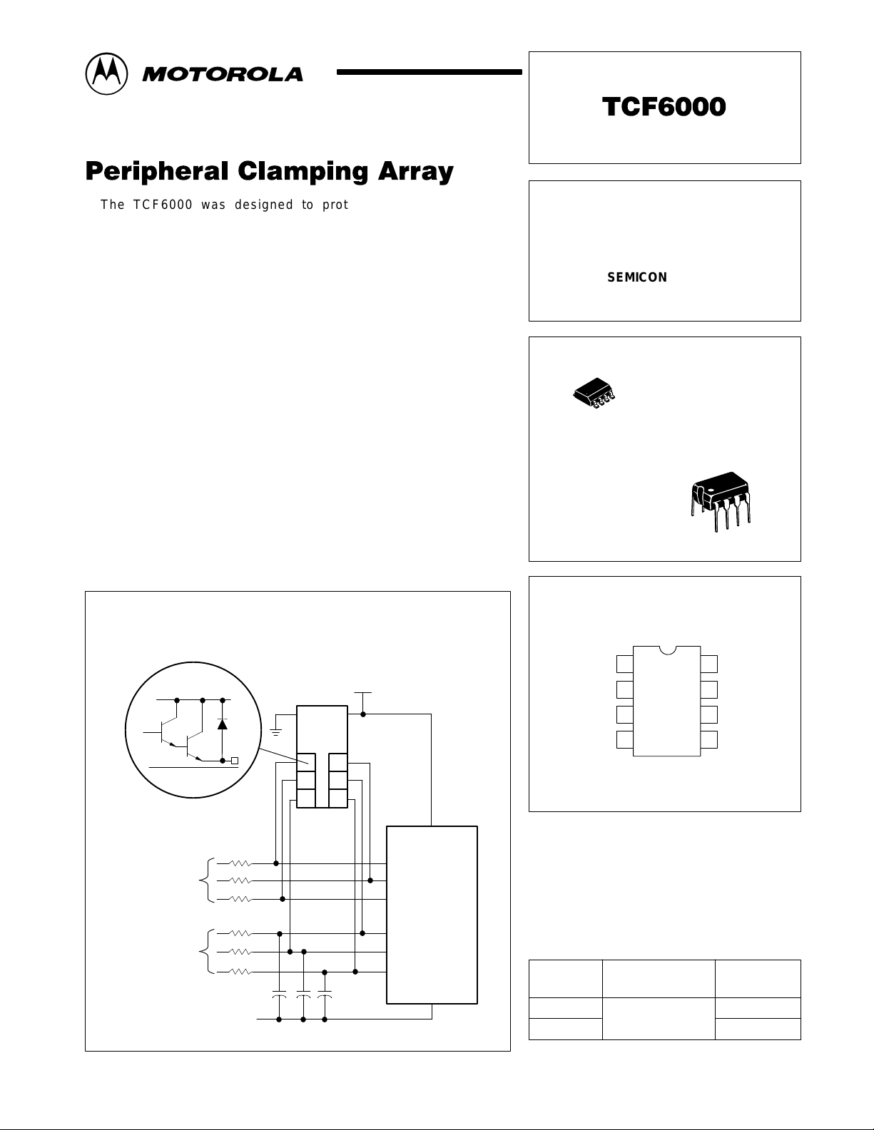
The TCF6000 was designed to protect input/output lines of
microprocessor systems against voltage transients.
• Optimized for HMOS System
• Minimal Component Count
• Low Board Space Requirement
• No P.C.B. Track Crossovers Required
• Applications Areas Include Automotive, Industrial,
Telecommunications and Consumer Goods
Figure 1. Representative Block Diagram and
Simplified Application
V
V
CC
V
Gnd
Ref
Generator
V
Ref
Pin
DD
PERIPHERAL CLAMPING
ARRAY
SEMICONDUCTOR
TECHNICAL DATA
D SUFFIX
PLASTIC PACKAGE
8
1
NO SUFFIX
PLASTIC PACKAGE
CASE 626
PIN CONNECTIONS
Gnd
1
2
Clamp
3
Clamp
45
Clamp
CASE 751
(SO–8)
V
8
CC
7
Clamp
6
Clamp
Clamp
Gnd
Each Cell
Digital
Inputs
Analog
Inputs
R
in
Gnd
MOTOROLA ANALOG IC DEVICE DATA
Micro
Computer
ORDERING INFORMATION
Operating
C
in
Device
TCF6000D
TCF6000
Motorola, Inc. 1996 Rev 0
Temperature Range
TA = – 40° to +85°C
Package
SO–8
Plastic DIP
1
TCF6000
MAXIMUM RATINGS
Supply Voltage V
Supply Current I
Clamping Current I
Junction Temperature T
Power Dissipation (TA = + 85°C) P
Thermal Resistance (Junction–Ambient) θ
Operating Ambient Temperature Range T
Storage Temperature Range T
NOTE: 1. Values beyond which damage may occur .
ELECTRICAL CHARACTERISTICS (T
Positive Clamping Voltage (Note 2)
(IIK = 10 mA, –40°C ≤ TA ≤ + 85°C)
Positive Peak Clamping Current I
Negative Peak Clamping Voltage
(IIK = –10 mA, –40°C ≤ TA ≤ + 85°C)
Negative Peak Clamping Current I
Output Leakage Current
(0 V ≤ Vin ≤ VCC)
(0 V ≤ Vin ≤ VCC, –40°C ≤ TA ≤ + 85°C)
Channel Crosstalk (ACT = 20 log IL/IIK) A
Quiescent Current (Package) I
NOTE: 2. The device might not give 100% protection in CMOS applications.
(TA = 25°C, unless otherwise noted, Note 1.)
Rating
Characteristics
Symbol Value Unit
CC
i
IK
J
D
JA
A
stg
= 25°C, 4.5 ≤ VCC ≤ 5.5 V, unless otherwise noted.)
A
6.0 V
300 mA
±50 mA
150 °C
400 m/W
100 °C/W
–40 to +85 °C
–55 to + 150 °C
Symbol Min Max Unit
V
(IK)
IK(P)
V
(IK)
IK(P)
I
L
I
LT
CT
B
– VCC + 1.0 V
– 20 mA
–0.3 – V
–20 – mA
–
–
100 – dB
– 2.0 mA
1.0
5.0
µA
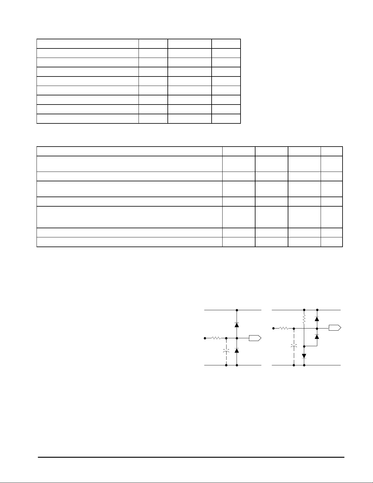
CIRCUIT DESCRIPTION
To ensure the reliable operation of any integrated circuit
based electronics system, care has been taken that voltage
transients do not reach the device I/O pins. Most NMOS,
HMOS and Bipolar integrated circuits are particularly
sensitive to negative voltage peaks which can provoke
latch–up or otherwise disturb the normal functioning of the
circuit, and in extreme cases may destroy the device.
Generally the maximum rating for a negative voltage
transients on integral circuits is –0.3 V over the whole
temperature range. Classical protection units have consisted
of diode/resistor networks as shown in Figures 2a and 2b.
The arrangement in Figure 2a does not, in general, meet
the specification and is therefore inadequate.
The problem with the solution shown if Figure 2b lies
mainly with the high current drain through the biassing
devices R1 and D3. A second problem exists if the input line
carries an analog signal. When Vin is close to the ground
potential, currents arising from leakage and mismatch
between D3 and D2 can be sourced into the input line, thus
disturbing the reading.
Figure 2. Classical Protection Circuits
(a) (b)
VinR
V
CC
D1
in
C
in
µ
D2
Gnd Gnd
VinR
C
R1
in
C
in
V
CC
D1
µ
C
D2
D
3
Figure 3 shows the clamping characteristics which
are common to each of the six cells in the Peripheral
Clamping Array.
As with the classical protection circuits, positive voltage
transients are clamped by means of a fast diode to the V
supply line.
CC
2
MOTOROLA ANALOG IC DEVICE DATA
 Loading...