

Motorola TCA5600 Datasheet
Order this document by TCA5600/D
The TCA5600, TCF5600 are versatile power supply control circuits for
microprocessor based systems and are mainly intended for automotive
applications and battery powered instruments. To cover a wide range of
applications, the devices offer high circuit flexibility with a minimum of
external components.
Functions included in this IC are a temperature compensated voltage
reference, on–chip dc/dc converter, programmable and remote controlled
voltage regulator, fixed 5.0 V supply voltage regulator with external PNP
power device, undervoltage detection circuit, power–on RESET delay and
watchdog feature for safe and hazard free microprocessor operations.
• 6.0 V to 30 V Operation Range
• 2.5 V Reference Voltage Accessible for Other Tasks
• Fixed 5.0 V ± 4% Microprocessor Supply Regulator Including Current
Limitation, Overvoltage Protection and Undervoltage Monitor.
• Programmable 6.0 V to 30 V Voltage Regulator Exhibiting High Peak
Current (150mA), Current Limiting and Thermal Protection.
• Two Remote Inputs to Select the Regulator’s Operation Mode:
OFF = 5.0 V, 5.0 V Standby
Programmable Output Voltage
• Self–Contained dc/dc Converter Fully Controlled by the Programmable
Regulator to Guarantee Safe Operation Under All Working Conditions
• Programmable Power–On RESET Delay
• Watchdog Select Input
• Negative Edge Triggered W atchdog Input
• Low Current Consumption in the V
• All Digital Control Ports are TTL and MOS–Compatible
Applications Include:
• Microprocessor Systems with E
• High Voltage Crystal and Plasma Displays
• Decentralized Power Supplies in Computer Telecom Systems
CC1
2
PROMs
Standby Mode
UNIVERSAL
MICROPROCESSOR POWER
SUPPLY/CONTROLLERS
SEMICONDUCTOR
TECHNICAL DATA
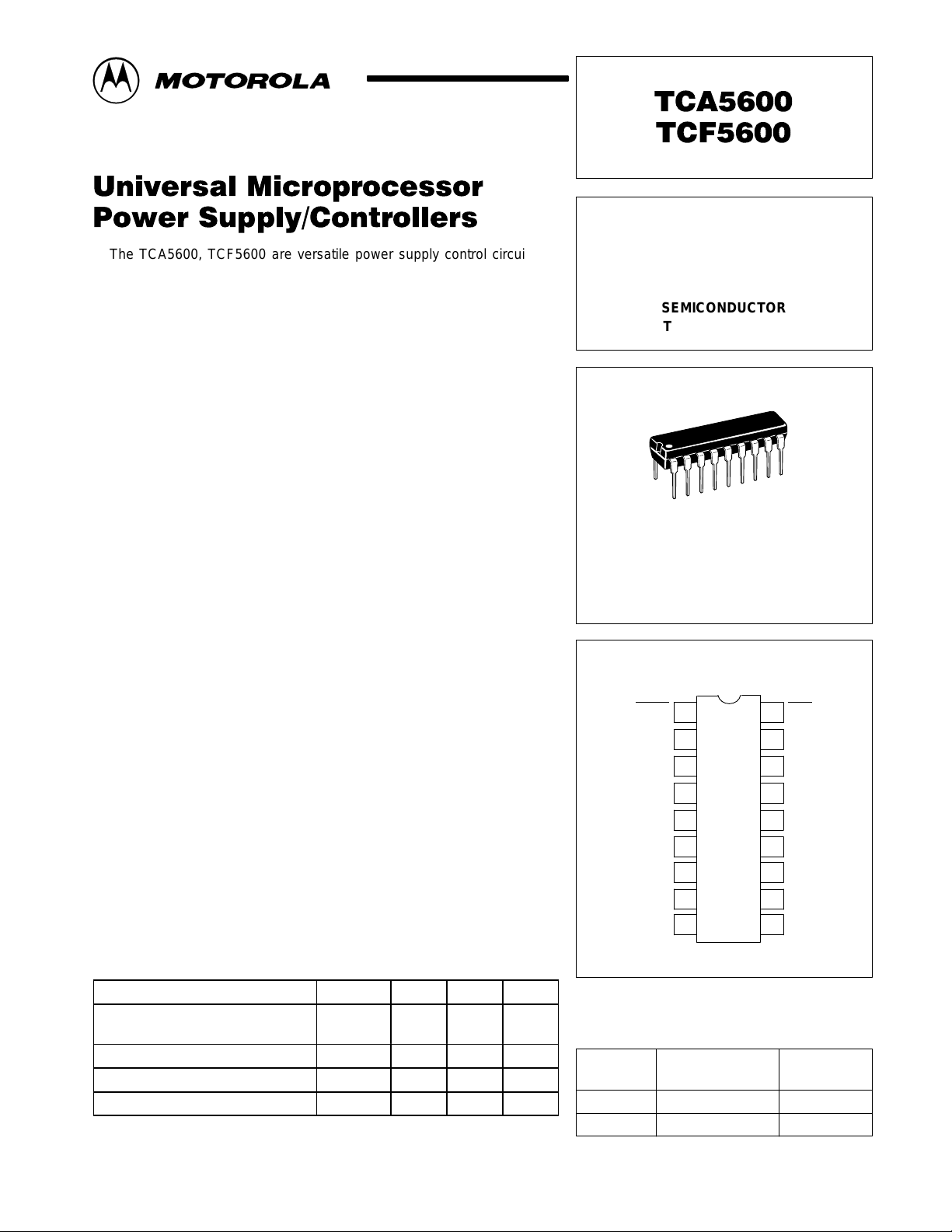
18
1
PLASTIC PACKAGE
CASE 707
PIN CONNECTIONS
RESET
V
Sense
out1
V
CC1
WDI
V
ref
INH1
V
Prog
out2
V
Output
out2
Converter Output
1
2
3
4
5
6
7
8
9
WDS
18
Delay
17
I
Sense
16
out1
Base Drive
15
V
14
CC2
GND
13
Current Sense
12
INH2
11
Converter Input
10
RECOMMENDED OPERATING CONDITIONS
Characteristics Symbol Min Max Unit
Power Supply Voltage V
Collector Current I
Output Voltage V
Reference Source Current I
V
CC1
CC2
C
out2
ref
MOTOROLA ANALOG IC DEVICE DATA
5.0
5.5
— 800 mA
6.0 30 V
0 2.0 mA
30
30
(Top View)
V
ORDERING INFORMATION
Operating
Device
TCA5600
TCF5600
Motorola, Inc. 1996 Rev 0
Temperature Range
TJ = 0° to +125°C
TJ = – 40° to +150°C
Package
Plastic DIP
Plastic DIP
1
MAXIMUM RATINGS
Power Supply Voltage (Pin 3,14) V
Base Drive Current (Pin 15) I
Collector Current (Pin 10) I
Forward Rectifier Current (Pin 10 to Pin 9) I
Logic Inputs INH1, INH2, WDS
(Pin 6, 11, 18)
Logic Input Current WDI (Pin 4) I
Output Sink Current RESET (Pin 1) I
Analog Inputs (Pin 2)
Analog Inputs (Pin 7)
Reference Source Current (Pin 5) I
Power Dissipation (Note 2)
TA = +75°C TCA5600
TA = +85°C TCF5600
Thermal Resistance, Junction–to–Air R
Operating Ambient Temperature Range
TCA5600
TCF5600
Operating Junction Temperature Range
TCA5600
TCF5600
Storage Temperature Range T
NOTES: 1. Values beyond which damage may occur.
2.Derate at 10 mW/°C for junction temperature above +75°C (TCA5600).
Derate at 10 mW/°C for junction temperature above +85°C (TCF5600).
(TA = +25°C [Note 1], unless otherwise noted.)
Rating Symbol Value Unit
CC1
V
WDI
RES
P
TCA5600 TCF5600
, V
B
C
F
INP
ref
D
θJA
T
A
T
stg
CC2
J
35 Vdc
20 mA
1.0 A
1.0 A
–0.3 V to V
–0.3 to 5.0
–40 to +85
–65 to +150 °C
CC1
±0.5 mA
10 mA
–0.3 to 10
5.0 mA
500
650
100 °C/W
0 to +75
+125
+150
Vdc
V
mW
°C
°C
Inhibit 2
(INH2)
Inhibit 1
(INH1)
Supply
Voltage V
RESET
CC1
11
6
3
1
Comp. II
Representative Block Diagram
CC2
Converter
Input
Converter
Output
Current
Sense VProgramming
10 9 12 7 8 14 16
DC/DC
Converter
Reference
2.5V
Delay Circuit
17
Delay
out2
A2
Thermal
Shut–Down
Watchdog
WDS
WDI
out2
Regulator
V
Comp. I
Supply
Voltage V
Current
Limit
Current
Sense
135418
ref
V
A1
A1
Gnd
Voltage
Protection
15
PNP Base Drive
2
V
Sense
out1
2
MOTOROLA ANALOG IC DEVICE DATA
TCA5600 TCF5600
ELECTRICAL CHARACTERISTICS (V
Characteristics
= V
CC1
= 12 V; TJ = 25°C; I
CC2
INH2 = High; WDS
= High; I
= 0 [Note 4]; unless otherwise noted.)
out2
Figure Symbol Min Typ Max Unit
ref
REFERENCE SECTION
Nominal Reference Voltage 1 V
Reference Voltage
I
= 0.5 mA, T
ref
Line Regulation (6.0 V ≤ V
Average Temperature Coefficient
T
≤ TJ ≤ T
low
Ripple Rejection Ratio
f = 1.0 kHz, V
low
high
sin
≤ TJ ≤ T
(Note 5)
= 1.0 V
(Note 5), 6.0 V ≤ V
high
≤ 18 V) Reg
CC2
CC1
≤ 18 V
2 ∆V
3 RR 60 70 — dB
pp
Output Impedance
0 ≤ I
≤ 2.0 mA
ref
Standby Current Consumption
V
= Open
CC2
4 I
5.0 V MICROPROCESSOR VOLTAGE REGULATOR SECTION
Nominal Output Voltage V
Output Voltage
5.0 mA ≤ I
6.0 V ≤ V
Line Regulation (6.0 V ≤ V
Load Regulation (5.0 mA ≤ I
Base Current Drive (V
Ripple Rejection Ratio
f = 1.0 kHz, V
out1
CC2
≤ 18 V
sin
≤ 300 mA, T
CC2
= 6.0 V, V15 = 4.0 V) I
CC2
= 1.0 V
pp
low
≤ TJ ≤ T
high
(Note 5)
5
6
≤ 18 V) Reg
≤ 300 mA) Reg
out1
3 RR 50 65 — dB
Undervoltage Detection Level (RSC = 5.0 Ω) 7 V
Current Limitation Threshold (RSC = 5.0 Ω) V
Average Temperature Coefficient
T
low
≤ TJ ≤ T
high
(Note 5)
DC/DC CONVERTER SECTION
Collector Current Detection Level High
9 V12(H)
RC = 10 k Low
Collector Saturation Voltage
10 V
IC = 600 mA (Note 6)
Rectifier Forward Voltage Drop
11 V
IF = 600 mA (Note 6)
NOTES: 3. The external PNP power transistor satisfies the following minimum specifications:
hFE ≥ 60 at IC = 500 mA and VCE = 5.0 V;
V
≤ 300 mV at IB = 10 mA and IC = 300 mA
CE(sat)
4.Regulator V
5.T
= 0°C for TCA5600 T
low
T
= +125°C for TCA5600 T
high
6.Pulse tested tp ≤ 300 µs.
programmed for nominal 24 V output by means of R4, R5 (see Figure 1).
out2
= –40°C for TCF5600
low
= +150°C for TCF5600
high
= 0; I
out1
ref nom
V
ref
line
ref
∆T
J
Z
O
CC1
out1(nom)
V
out1
line
load
B
low
RSC
∆V
out1
∆T
J
V12(L)
CE(sat)
F
= 0 [Note 3]; RSC = 0.5 Ω; INH = High
2.42 2.5 2.58 V
2.4 — 2.6 V
— 2.0 15 mV
— — ±0.5 mV/°C
— 1.0 — Ω
— 3.0 — mA
4.8 5.0 5.2 V
4.75 — 5.25 V
— 10 50 mV
— 20 100 mV
10 15 — mA
4.5 0.93 × V
out1
— V
210 250 290 mV
— — ±1.0 mV/°C
350
—
400
50
450
—
— — 1.6 V
— — 1.4 V
mV
MOTOROLA ANALOG IC DEVICE DATA
3
TCA5600 TCF5600
ELECTRICAL CHARACTERISTICS
ELECTRICAL CHARACTERISTICS INH2 = High; WDS = High; I
Characteristics
(V
CC1
= V
= 12 V; TJ = 25°C; I
CC2
ref
= 0 [Note 4]; unless otherwise noted.)
out2
Symbol Min Typ Max Unit
PROGRAMMABLE VOLTAGE REGULATOR SECTION (Note 6)
Nominal Output Voltage V
Output Voltage (Figure 8)
1.0 mA ≤ I
Load Regulation 1.0 mA ≤ I
≤ 100 mA, T
out2
≤ TJ ≤ T
low
≤ 100 mA (Note 7) Reg
out2
(Notes 5, 7)
high
out2(nom)
V
DC Output Current I
Peak Output Current (Internally Limited) I
out2 p
Ripple Rejection Ratio
f = 20 kHz, V = 0.4 V
Output Voltage (Fixed 5.0 V)
1.0 mA ≤ I
INH1 = HIGH (Note 5)
out2
pp
≤ 20 mA, T
low
≤ TJ ≤ T
high
V
out2(5.0 V)
Off State Output Impedance (INH2 = Low) R
Average Temperature Coefficient
T
low
≤ TJ ≤ T
high
(Note 5)
∆V
∆TJV
WATCHDOG AND RESET CIRCUIT SECTION
Threshold Voltage High
(Static) Low
Current Source T
Power–Up RESET
low
≤ TJ ≤ T
high
(Note 5)
V
V
Watchdog Time Out
Watchdog RESET
Watchdog Input V oltage Swing V
Watchdog Input Impedance r
Watchdog Reset Pulse Width (C8 = 1.0 nF) (Note 9) t
DIGITAL PORTS: WDS, INH 1, INH 2, RESET (Note 8)
Input Voltage Range V
Input High Current
2.0 V ≤ VIH ≤ 5.5 V
5.5 V ≤ VIH ≤ V
CC1
Input Low Current
–0.3 V ≤ VIL ≤ 0.8 V for INH1, INH2, –0.3 V ≤ VIL ≤ 0.4 V for WDS
Leakage Current Immunity (INH2, High “Z” State) (Figure 12) I
Output Low Voltage RESET (IOL = 6.0 mA) V
Output High Voltage RESET (VOH = 5.5 V) V
NOTES: 3. The external PNP power transistor satisfies the following minimum specifications:
hFE ≥ 60 at IC = 500 mA and VCE = 5.0 V;
V
≤ 300 mV at IB = 10 mA and IC = 300 mA
CE(sat)
4.Regulator V
5.T
= 0°C for TCA5600 T
low
T
= +125°C for TCA5600 T
high
6.V9 = 28 V, INH1 = LOW for this Electrical Characteristic section unless otherwise noted.
7.Pulse tested tp ≤ 300 µs.
8.Temperature range T
9.For test purposes, a negative pulse is applied to Pin 4 (–2.5 V ≥ V4 ≥ –5.5 V).
programmed for nominal 24 V output by means of R4, R5 (see Figure 1).
out2
low
≤ TJ ≤ T
= –40°C for TCF5600
low
= +150°C for TCF5600
high
applies to this Electrical Characteristics section.
high
= 0; I
= 0 [Note 3]; RSC = 0.5 Ω; INH = High
out1
23 24 25 V
out2
load
out2
22.8 — 25.2 V
— 40 200 mV
100 — — mA
150 200 — mA
RR 45 55 — dB
4.75 — 5.25 V
out1
out2
— 10 — kΩ
— — ±0.25 mV/°C V
out2
C5(H)
C5(L)
I
C5
WDI
i
p
INP
I
IH
I
IL
Z
OL
OH
—
—
–1.8
—
—
— — ±5.5 V
12 15 — kΩ
— — 10 µs
— — –0.3 to V
—
—
— — –100
±20 — — µA
— — 0.4 V
— — 20 µA
2.5
1.0
–2.5
5×I
–50×I
—
—
C5
C5
—
—
–3.2
—
—
CC1
100
150
V
µA
V
µA
µA
4
MOTOROLA ANALOG IC DEVICE DATA
 Loading...