

Motorola TCA3388DP, TCA3388FP Datasheet
Order this document by TCA3388/D
The TCA3388 is a telephone line interface circuit which performs the basic
functions of a telephone set in combination with a microcontroller and a ringer.
It includes dc and ac line termination, the hybrid function with 2 adjustable
sidetone networks, handset connections and an efficient supply point.
FEATURES
Line Driver and Supply
• DC and AC Termination of the Telephone Line
• Selectable DC Mask: France, U.K., Low Voltage
• Current Protection
• Adjustable Set Impedance for Resistive and Complex Termination
• Efficient Supply Point for Peripherals
• Hook Status Detection
Handset Operation
• Transmit and Receive Amplifiers
• Double Anti–Sidetone Network
• Line Length AGC
• Microphone and Earpiece Mute
• Transmit Amplifier Soft Clipping
Dialing and Ringing
• Interrupter Driver for Pulse–Dialing
• Reduced Current Consumption During Pulse–Dialing
• DTMF Interfacing
• Ringing via External Ringer
TELEPHONE LINE
INTERFACE
SEMICONDUCTOR
TECHNICAL DATA
20
1
DP SUFFIX
PLASTIC PACKAGE
CASE 738
20
1
FP SUFFIX
PLASTIC PACKAGE
CASE 751D
PIN CONNECTIONS
Application Areas
• Corded Telephony
• Cordless Telephony Base Station
• Answering Machines
• Fax
• Intercom
• Modem
This document contains information on a new product. Specifications and information herein
are subject to change without notice.
MOTOROLA ANALOG IC DEVICE DATA
120
RXI
2
TXI
3
Mic
4
LAO
5
LAI
6
HYL
7
HYS
8
CM
9
IMP
SAO SAI
ORDERING INFORMATION
Device
TCA3388DP
TCA3388FP
Motorola, Inc. 1995
Temperature Range
(Top View)
Tested Operating
TA = 0° to +70°C
19
18
17
16
15
14
13
12
1110
RXO2
RXO1
Gnd
V
CC
I
ref
MUT
PI
HSO
DCM
Package
DIP
SOIC
1
TCA3388
ÁÁÁ
ÁÁÁ
ÁÁÁ
ÁÁÁ
ÁÁÁ
ÁÁÁ
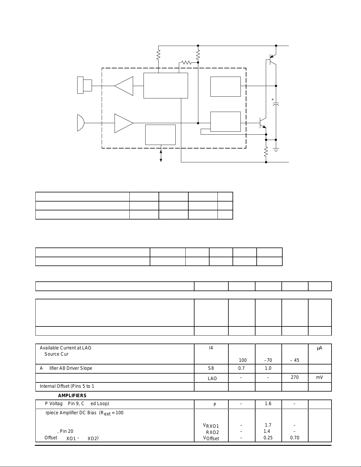
Simplified Block Diagram
DC and AC
Termination
Line +
Handset
Earpiece
Handset
MIcrophone
Ear
Mic
DC Mask Generation
AC Termination
2–4 Wire Conversion
Microcontroller
Interface
This device contains 1,911 active transistors.
MAXIMUM RATINGS
Rating Symbol Min Max Unit
Maximum Junction Temperature T
Storage Temperature Range T
NOTE: Devices should not be operated at or outside these values. The “Recommended Operating
Limits” provide for actual device operation.
J
stg
– +150 °C
–65 +150 °C
RECOMMENDED OPERATING CONDITIONS
Characteristic Symbol Min Typ Max Unit
Operating Temperature Range T
A
0 – +70 °C
Supply
Stabilizer
Line Driver
Line –
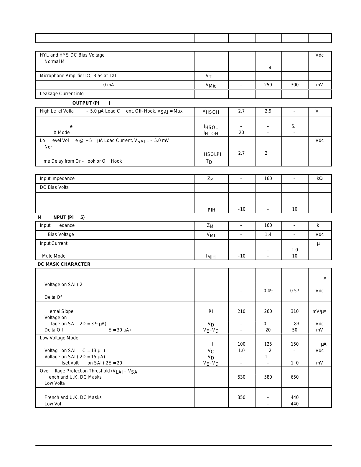
DC ELECTRICAL CHARACTERISTICS (T
Characteristic
= 25°C)
A
Symbol Min Typ Max Unit
VOLTAGE REGULATOR
Regulated Supply at Pin 17 V
CC
ICC = 7.0 mA 3.4 3.7 4.0
ICC = 20 mA 3.45 3.75 4.05
ICC = 80 mA 3.5 3.8 4.1
Current Consumption at Pin 17, Pin PI = High I
CC
– – 600 µA
DRIVER DC CHARACTERISTICS
Available Current at LAO
I4
Source Current 45 70 100
Sink Current –100 –70 –45
Amplifier A8 Driver Slope
LAO Voltage (PI = High, I4 = 100 µA)
Internal Offset (Pins 5 to 10)
S8
V
LAO
VO1–VO2
0.7
30
1.0
–
–
80
SPEECH AMPLIFIERS
IMP Voltage (Pin 9, Closed Loop)
Earpiece Amplifier DC Bias (R
= 100 kΩ)
ext
RXI, Pin 1 V
RXO1 Pin 19 V
RXO2, Pin 20 V
Offset (V
RXO1
– V
) V
RXO2
V
IMP
RXI
RXO1
RXO2
Offset
–
1.6
– 1.6 –
– 1.7 –
– 1.45 –
– 0.25 0.70
1.2
270
140
–
Vdc
µA
µA/mV
mV
mV
Vdc
Vdc
2
MOTOROLA ANALOG IC DEVICE DATA
TCA3388
ÁÁÁ
ÁÁÁ
ÁÁÁ
ÁÁÁ
ÁÁÁ
ÁÁÁ
ÁÁÁ
ÁÁÁ
ÁÁÁ
ÁÁÁ
ÁÁÁ
ÁÁÁ
ÁÁÁ
ÁÁÁ
ÁÁÁ
ÁÁÁ
ÁÁÁ
ÁÁÁ
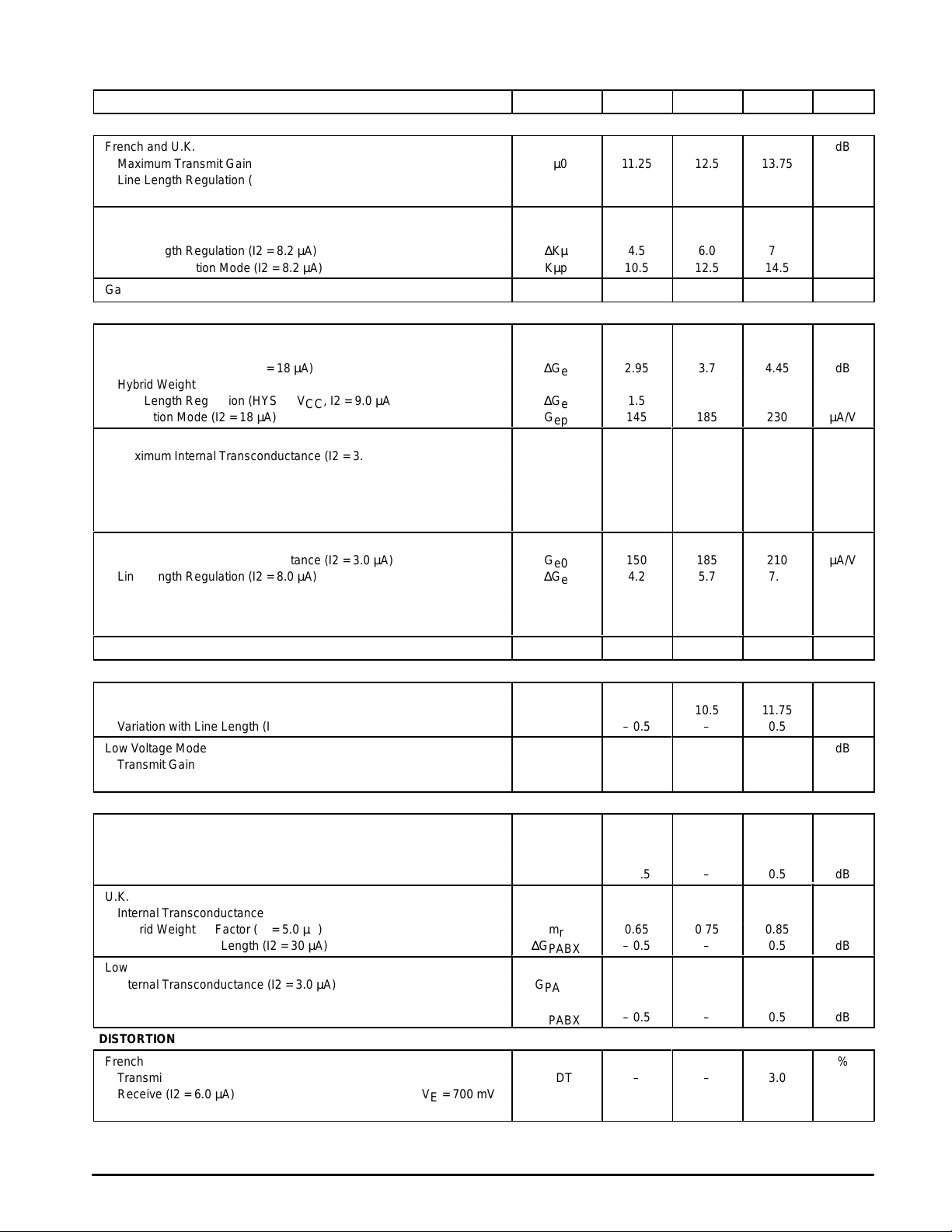
DC ELECTRICAL CHARACTERISTICS (continued) (T
= 25°C)
A
Characteristic UnitMaxTypMinSymbol
SPEECH AMPLIFIERS
HYL and HYS DC Bias Voltage
Normal Mode V
PI = High V
Microphone Amplifier DC Bias at TXI
Saturation Voltage at Mic @ 1.0 mA
Leakage Current into Mic @ 3.7 V
HY1
HY2
V
TXI
V
Mic
I
Leak
– 2.4 –
– 1.4 –
–
–
–
1.45
250
–
300
–
2.0
HOOK STATUS OUTPUT (Pin 13)
High Level Voltage @ – 5.0 µA Load Current, Off–Hook, V
SAI
= Max
V
HSOH
2.7
2.9
–
Maximum Load Current
Normal Mode I
PABX Mode I
Low Level Voltage @ + 5.0 µA Load Current, V
= – 5.0 mV
SAI
Normal On–Hook V
PI = High V
Time Delay from On–Hook or Off–Hook
HSOL
HSOH
HSOL
HSOLPI
T
Del
– – 5.0
20 – –
– – 0.60
2.7 2.9 –
–
3.5
–
PULSE INPUT (Pin 14)
Input Impedance
DC Bias Voltage
Z
PI
V
PIL
–
–
160
1.4
–
–
Input Current
Make Phase I
Break Phase I
PIL
PIH
–1.0 – 1.0
–10 – 10
MUTE INPUT (Pin 15)
Input Impedance
DC Bias Voltage
Z
MI
V
MI
–
–
160
1.4
–
–
Input Current
Speech Mode I
Mute Mode I
MIL
MIH
–1.0 – 1.0
–10 – 10
DC MASK CHARACTERISTICS
French
Internal Slope RI 120 160 200 mV/µA
Voltage on SAI (I2C = 3.6 µA) V
Voltage on SAI (I2D = 4.0 µA) V
C
D
Delta Offset Voltage on SAI (I2E = 30 µA) VE–V
D
0.40 0.47 – Vdc
– 0.49 0.57 Vdc
– – 30 mV
U.K.
Internal Slope RI 210 260 310 mV/µA
Voltage on SAI (I2C = 3.5 µA) V
Voltage on SAI (I2D = 3.9 µA) V
C
D
Delta Offset Voltage on SAI (I2E = 30 µA) VE–V
D
0.59 0.70 – Vdc
– 0.72 0.83 Vdc
– 20 50 mV
Low Voltage Mode
Internal Slope RI 100 125 150 mV/µA
Voltage on SAI (I2C = 13 µA) V
Voltage on SAI (I2D = 15 µA) V
Delta Offset Voltage on SAI (I2E = 20 µA) VE–V
Overvoltage Protection Threshold (V
LAI
– V
SAO
)
V
C
D
D
Clamp1
1.0 1.2 – Vdc
– 1.3 1.55 Vdc
– – 100 mV
French and U.K. DC Masks 530 580 650
Low Voltage DC Mask 280 – 385
Protection Voltage Level (V
LAI
– V
SAO
)
V
Clamp2
French and U.K. DC Masks 350 – 440
Low Voltage DC Mask 280 – 440
Vdc
Vdc
mV
µA
Vdc
µA
Vdc
ms
kΩ
Vdc
µA
kΩ
Vdc
µA
mV
mV
MOTOROLA ANALOG IC DEVICE DATA
3
TCA3388
ÁÁÁ
ÁÁÁ
ÁÁÁ
ÁÁÁ
ÁÁÁ
ÁÁÁ
ÁÁÁ
ÁÁÁ
ÁÁÁ
ÁÁÁ
ÁÁÁ
ÁÁÁ
ÁÁÁ
AC ELECTRICAL CHARACTERISTICS
Characteristic
(TA = 25°C)
Symbol Min Typ Max Unit
TRANSMIT MODE
French and U.K.
Maximum Transmit Gain (I2 = 3.0 µA) Kµ0 11.25 12.5 13.75
Line Length Regulation (I2 = 30 µA) ∆Kµ 5.5 6.5 7.5
Gain in Protection Mode (I2 = 30 µA) Kµp 10.5 12.5 14.5
Low Voltage Mode
Maximum Transmit Gain (I2 = 3.0 µA) Kµ0 11.25 12.5 13.75
Line Length Regulation (I2 = 8.2 µA) ∆Kµ 4.5 6.0 7.5
Gain in Protection Mode (I2 = 8.2 µA) Kµp 10.5 12.5 14.5
Gain Reduction when Microphone is Muted
∆Kµm
60
–
RECEIVE MODE
French
Maximum Internal Transconductance (I2 = 3.0 µA) G
Line Length Regulation (I2 = 18 µA) ∆G
Hybrid Weighting Factor (I2 = 18 µA) m
Line Length Regulation (HYS @ VCC, I2 = 9.0 µA) ∆G
Protection Mode (I2 = 18 µA) G
e0
e
r
e
ep
150 180 210 µA/V
2.95 3.7 4.45 dB
0.4 0.5 0.6
1.5 2.1 2.5 dB
145 185 230 µA/V
U.K.
Maximum Internal Transconductance (I2 = 3.0 µA) G
Line Length Regulation (I2 = 18 µA) ∆G
Hybrid Weighting Factor (I2 = 13 µA) m
Line Length Regulation (HYS @ VCC, I2 = 9.0 µA) ∆G
Protection Mode (I2 = 18 µA) G
e0
e
r
e
ep
150 180 210 µA/V
2.8 3.5 4.3 dB
0.4 0.5 0.6
1.4 1.9 2.4 dB
145 185 230 µA/V
Low Voltage Mode
Maximum Internal Transconductance (I2 = 3.0 µA) G
Line Length Regulation (I2 = 8.0 µA) ∆G
Hybrid Weighting Factor (I2 = 7.0 µA) m
Line Length Regulation (HYS @ VCC, I2 = 4.0 µA) ∆G
Protection Mode (I2 = 8.0 µA) G
Earpiece Gain Reduction when Muted
∆G
e0
e
r
e
ep
em
150 185 210 µA/V
4.2 5.7 7.2 dB
– 0.5 –
– 3.0 – dB
145 185 230 µA/V
60
–
TRANSMIT PABX MODE
French and U.K.
Transmit Gain (I2 = 3.0 µA) K
Variation with Line Length (I2 = 30 µA) ∆K
PABX
PABX
9.25 10.5 11.75
– 0.5 – 0.5
Low Voltage Mode
Transmit Gain (I2 = 3.0 µA) K
Variation with Line Length (I2 = 30 µA) ∆K
PABX
PABX
9.25 10.5 11.75
– 0.5 – 0.5
RECEIVE PABX MODE
French
Internal Transconductance (I2 = 5.0 µA) G
Hybrid Weighting Factor (I2 = 5.0 µA) m
Variation with Line Length (I2 = 30 µA) ∆G
U.K.
БББББББББББББББББ
Internal Transconductance (I2 = 5.0 µA) G
Hybrid Weighting Factor (I2 = 5.0 µA) m
Variation with Line Length (I2 = 30 µA) ∆G
Low Voltage Mode
БББББББББББББББББ
Internal Transconductance (I2 = 3.0 µA) G
Hybrid Weighting Factor (I2 = 3.0 µA) m
Variation with Line Length (I2 = 30 µA) ∆G
PABX
r
PABX
ÁÁÁ
PABX
r
PABX
ÁÁÁ
PABX
r
PABX
120 145 170 µA/V
0.8 0.9 1.0
– 0.5 – 0.5 dB
ÁÁ
120 145 170 µA/V
ÁÁ
0.65 0.75 0.85
– 0.5 – 0.5 dB
ÁÁ
120 145 170 µA/V
ÁÁ
– 0.9 –
– 0.5 – 0.5 dB
DISTORTION
French
Transmit (I2 = 10 µA) THDT – – 3.0
Receive (I2 = 6.0 µA) VE = 700 mV THDR – – 3.0
VE = 1250 mV – – 5.0
NOTE:VE is the differential earpiece voltage across Pins 19 and 20.
–
–
ÁÁ
ÁÁ
dB
dB
dB
dB
dB
dB
ÁÁ
ÁÁ
%
4
MOTOROLA ANALOG IC DEVICE DATA
TCA3388
ÁÁÁ
Á
Á
Á
Á
Á
Á
Á
Á
Á
Á
Á
Á
Á
Á
Á
AC ELECTRICAL CHARACTERISTICS (continued) (T
= 25°C)
A
Characteristic UnitMaxTypMinSymbol
DISTORTION
Low Voltage
Transmit (I2 = 10 µA) THDT – – 3.0
Receive (I2 = 6.0 µA) VE = 700 mV THDR – – 3.0
VE = 1250 mV – – 5.0
NOTE:VE is the differential earpiece voltage across Pins 19 and 20.
TYPICAL TEMPERATURE PERFORMANCE
Characteristic Typical Value @ 25°C Typical Change – 20 to + 60°C
VCC Regulated Supply @ Pin 17
Current Consumption at Pin 17, Pin PI = High
Amplifier A8 Driver Slope
Voltage on SAI V
ББББББББББББ
ББББББББББББ
C
БББББББББ
V
D
БББББББББ
Internal Slope for Low Voltage Mode
Transmit Gain Kµ0
Line Length Regulation ∆Kµ French
ББББББББББББ
ББББББББББББ
Internal Transconductance G
Line Length Regulation ∆G
ББББББББББББ
e0
e
French
NOTE: Temperature data is typical performance only, based on sample characterization, and does not provide guaranteed limits over temperature.
БББББББББ
U.K.
L.V .
БББББББББ
U.K.
БББББББББ
L.V .
3.7
400 µA
1.0 µA/mV
French = 0.47 Vdc
U.K. = 0.70 Vdc
French = 0.49 Vdc
U.K. = 0.72 Vdc
125 mV/µA
12.5 dB
6.5 dB
6.5 dB
6.0 dB
180 µA/V
3.7 dB
3.5 dB
5.7 dB
– 0.8 mV/°C
– 0.55 µA/°C
– 0.0035 µA/mV/°C
БББББББББ
БББББББББ
0.35 mV/°C
0.07 mV/µA/°C
0.01 dB/°C
< 0.3 dB Variation
БББББББББ
БББББББББ
< 0.3 dB Variation
– 0.05 dB/°C
< 1.0 dB Variation
< 0.5 dB Variation
< 0.5 dB Variation
БББББББББ
– 0.04 dB/°C
%
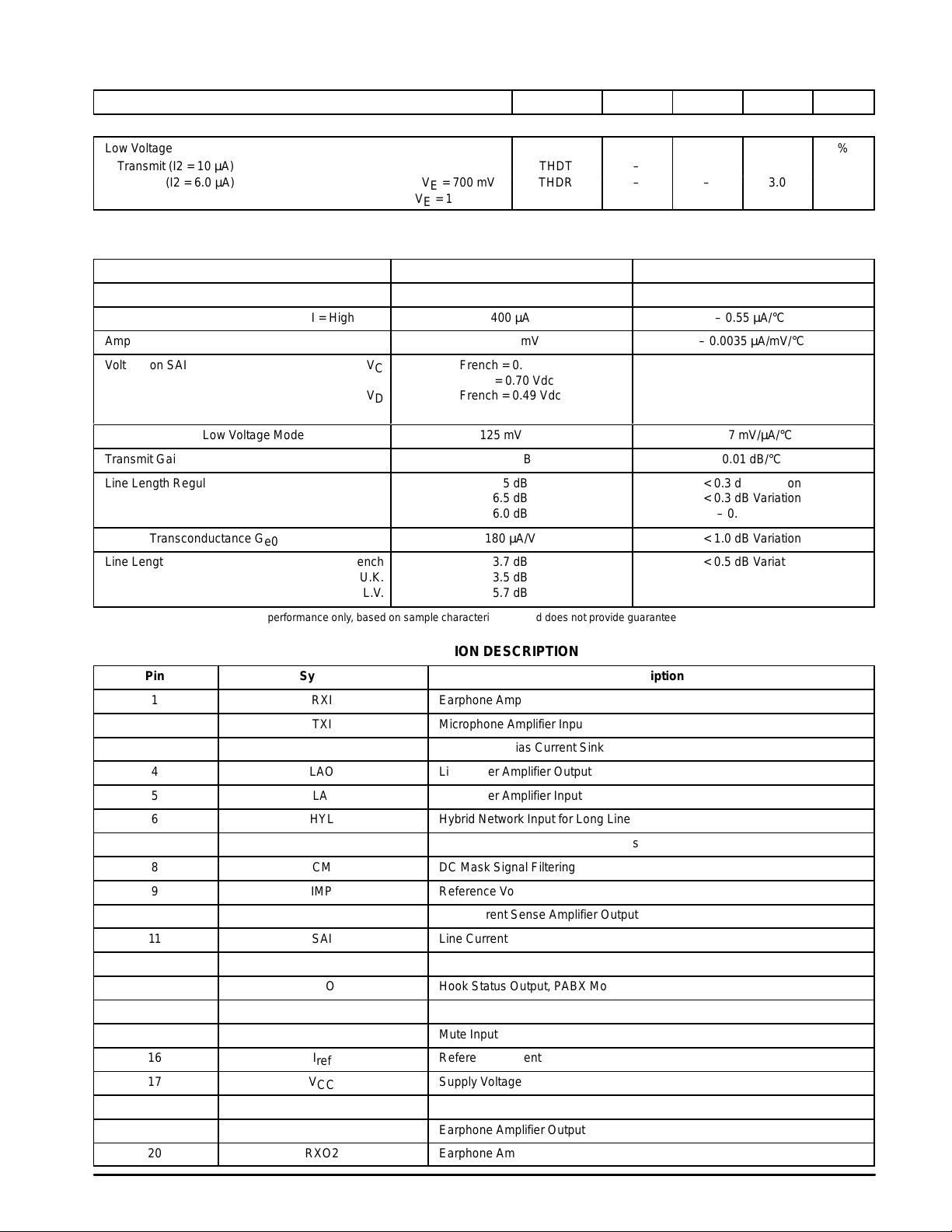
PIN FUNCTION DESCRIPTION
Pin Symbol Description
1 RXI Earphone Amplifier Input
2 TXI Microphone Amplifier Input
3 Mic Microphone Bias Current Sink
4 LAO Line Driver Amplifier Output
5 LAI Line Driver Amplifier Input
6 HYL Hybrid Network Input for Long Lines
7 HYS Hybrid Network Input for Short Lines
8 CM DC Mask Signal Filtering
9 IMP Reference Voltage
10 SAO Line Current Sense Amplifier Output
11 SAI Line Current Sense Amplifier Input
12 DCM DC Mask Select
13 HSO Hook Status Output, PABX Mode Select
14 PI Pulse Input
15 MUT Mute Input
16 I
17 V
ref
CC
18 Gnd Ground
19 RXO1 Earphone Amplifier Output
20 RXO2 Earphone Amplifier Inverted Output
Reference Current
Supply Voltage
MOTOROLA ANALOG IC DEVICE DATA
5
 Loading...