

MOTOROLA TCA0372DWR2, TCA0372DW, TCA0372DP2, TCA0372DP1, TCA0372DM2L2 Datasheet
...
Order this document by TCA0372/D
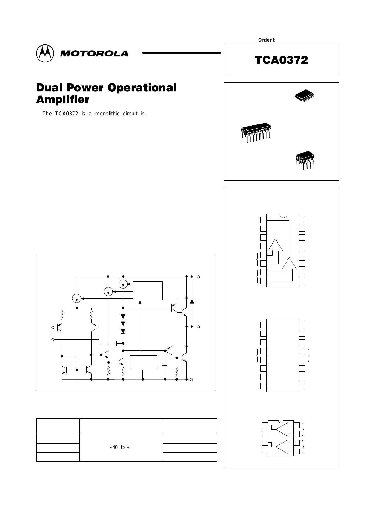
DP2 SUFFIX
PLASTIC PACKAGE
CASE 648
PIN CONNECTIONS
(Top View)
DW SUFFIX
PLASTIC PACKAGE
CASE 751G
SOP (12+2+2)L
1
16
16
1
TCA0372DW
TCA0372DP2
Output A
V
CC
Output B
VEE/Gnd
Inputs B
Inputs A
Gnd
Gnd
Gnd
Gnd
Gnd
Gnd
Gnd
Gnd
16
15
14
13
12
11
10
9
1
2
3
4
5
6
7
8
+
+
–
–
V
CC
Output B
NC
VEE/Gnd
Inputs –B
Inputs +B
NC
Output A
NC
NC
VEE/Gnd
Input –A
Input +A
NC
16
15
14
13
12
11
10
9
1
2
3
4
5
6
7
8
(Top View)
*Pins 4 and 9 to 16 are internally connected.
8
1
DP1 SUFFIX
PLASTIC PACKAGE
CASE 626
(Top View)
Output A
VEE/Gnd
+
–
TCA0372DP1
1
2
3
4
8
7
6
5
+
–
V
CC
Output B
Inputs A
Inputs B
1
MOTOROLA ANALOG IC DEVICE DATA
The TCA0372 is a monolithic circuit intended for use as a power
operational amplifier in a wide range of applications, including servo
amplifiers and power supplies. No deadband crossover distortion provides
better performance for driving coils.
• Output Current to 1.0 A
• Slew Rate of 1.3 V/µs
• Wide Bandwidth of 1.1 MHz
• Internal Thermal Shutdown
• Single or Split Supply Operation
• Excellent Gain and Phase Margins
• Common Mode Input Includes Ground
• Zero Deadband Crossover Distortion
Representative Block Diagram
V
EE
V
CC
Output
Thermal
Protection
Current
Bias
Monitoring
Inv.
Input
Noninv.
Input
ORDERING INFORMATION
Device
Operating
Temperature Range
Package
TCA0372DW
SOP (12+2+2) L
TCA0372DP1
TJ = –40° to +150°C
Plastic DIP
TCA0372DP2
Plastic DIP
Motorola, Inc. 1999 Rev 2
TCA0372
2
MOTOROLA ANALOG IC DEVICE DATA
MAXIMUM RATINGS
Rating Symbol Value Unit
Supply Voltage (from VCC to VEE) V
S
40 V
Input Differential Voltage Range V
IDR
(Note 1) V
Input Voltage Range V
IR
(Note 1) V
Junction Temperature (Note 2) T
J
+150 °C
Storage Temperature Range T
stg
–55 to +150 °C
DC Output Current I
O
1.0 A
Peak Output Current (Nonrepetitive) I
(max)
1.5 A
DC ELECTRICAL CHARACTERISTICS (V
CC
= +15 V , VEE = –15 V, RL connected to ground, TJ = –40° to +125°C.)
Characteristics
Symbol Min Typ Max Unit
Input Offset Voltage (VCM = 0)
TJ = +25°C
TJ, T
low
to T
high
V
IO
—
—
1.0
—
15
20
mV
Average Temperature Coefficient of Of fset Voltage ∆VIO/∆T — 20 — µV/°C
Input Bias Current (VCM = 0) I
IB
— 100 500 nA
Input Offset Current (VCM = 0) I
IO
— 10 50 nA
Large Signal Voltage Gain
VO = ±10 V, RL = 2.0 k
A
VOL
30 100 — V/mV
Output Voltage Swing (IL = 100 mA)
TJ = +25°C
TJ = T
low
to T
high
TJ = +25°C
TJ = T
low
to T
high
V
OH
V
OL
14.0
13.9
—
—
14.2
—
–14.2
—
—
—
–14.0
–13.9
V
Output Voltage Swing (IL = 1.0 A)
VCC = +24 V , VEE = 0 V, TJ = +25°C
VCC = +24 V , VEE = 0 V, TJ = T
low
to T
high
VCC = +24 V , VEE = 0 V, TJ = +25°C
VCC = +24 V , VEE = 0 V, TJ = T
low
to T
high
V
OH
V
OL
22.5
22.5
—
—
22.7
—
1.3
—
—
—
1.5
1.5
V
Input Common Mode Voltage Range
TJ = +25°C
TJ = T
low
to T
high
V
ICR
VEE to (VCC –1.0)
VEE to (VCC –1.3)
V
Common Mode Rejection Ratio (RS = 10 k) CMRR 70 90 — dB
Power Supply Rejection Ratio (RS = 100 Ω) PSRR 70 90 — dB
Power Supply Current
TJ = +25°C
TJ = T
low
to T
high
I
D
—
—
5.0
—
10
14
mA
NOTES: 1. Either or both input voltages should not exceed the magnitude of VCC or VEE.
2.Power dissipation must be considered to ensure maximum junction temperature (TJ) is not exceeded.
AC ELECTRICAL CHARACTERISTICS (V
CC
= +15 V , VEE = –15 V, RL connected to ground, TJ = +25°C, unless otherwise noted.)
Characteristics
Symbol Min Typ Max Unit
Slew Rate (Vin = –10 V to +10 V, RL = 2.0 k, CL = 100 pF)
AV = –1.0, TJ = T
low
to T
high
SR 1.0 1.4 — V/µs
Gain Bandwidth Product (f = 100 kHz, CL = 100 pF, RL = 2.0 k)
TJ = 25°C
TJ = T
low
to T
high
GBW
0.9
0.7
1.4
—
—
—
MHz
Phase Margin TJ = T
low
to T
high
RL = 2.0 k, CL = 100 pF
φ
m
— 65 — Degrees
Gain Margin
RL = 2.0 k, CL = 100 pF
A
m
— 15 — dB
Equivalent Input Noise Voltage
RS = 100 Ω, f = 1.0 to 100 kHz
e
n
— 22 —
nV/ Hz√
Total Harmonic Distortion
AV = –1.0, RL = 50 Ω, VO = 0.5 VRMS, f = 1.0 kHz
THD — 0.02 — %
NOTE: In case VEE is disconnected before VCC, a diode between VEE and Ground is recommended to avoid damaging the device.
TCA0372
3
MOTOROLA ANALOG IC DEVICE DATA
VCC = +15 V
VEE = –15 V
RL = 2.0 k
Ω
Figure 1. Supply Current versus Suppy Voltage
with No Load
Figure 2. Output Saturation Voltage
versus Load Current
Figure 3. Voltage Gain and Phase
versus Frequency
Figure 4. Phase Margin versus Output
Load Capacitance
Figure 5. Small Signal Transient Response Figure 6. Large Signal Transient Response
V
O
,OUTPUT VOLTAGE (50 mV/DIV)
t, TIME (1.0 µs/DIV)
V
O
, OUTPUT VOLTAGE (5.0 V/DIV)
t, TIME (10 µs/DIV)
, SUPPLY CURRENT (mA)I
CC
6.5
5.5
4.5
3.5
2.5
0 2.0 4.0 6.0 8.0 10 12 14 16 18 20
VCC, |VEE|, SUPPLY VOLTAGE (V)
0 1.00.5
IL, LOAD CURRENT (A)
, OUTPUT SA TURATION VOLTAGE (V)V
sat
80
40
20
–20
1.0 10 100 1000 10000
130
120
110
100
90
80
f, FREQUENCY (kHz)
PHASE (DEGREES)
GAIN (dB)
0.4
CL, OUTPUT LOAD CAPACITANCE (nF)
, PHASE MARGIN (DEGREES)
φ
m
60
70
50
40
30
20
0 0.8 1.2 1.6 2.0
VCC = +15 V
VEE = –15 V
RL = 2.0 k
Ω
AV = –100
VCC = 24 V
VEE = 0 V
60
VCC = +15 V
VEE = –15 V
AV = +1.0
RL = 2.0 k
Ω
VCC = +15 V
VEE = –15 V
AV = +1.0
RL = 2.0 k
Ω
V
CC
VCC–1.0
VCC–2.0
VCC+2.0
V
EE
VCC+1.0
 Loading...