

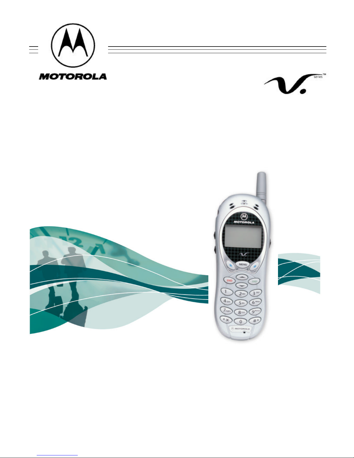
Motorola Tarpon V. 120C, 120c Service Manual
V.120c
Service Manual Level 3
Revision 01
Motorola V.series™ 120c
CDMA 800/1900/AMPS 800
© 2001 Motorola, Inc. 1

Computer Software Copyrights
V.120c
COMPUTER SOFTWARE COPYRIGHTS
The Motorola products described in this instruction manual may
include copyrighted Motorola computer programs stored in semiconductor memories or other media. Laws in the United States
and other countries preserve for Motorola certain exclusive rights
for copyrighted computer programs, including the exclusive right
to copy or reproduce in any form the copyrighted computer
program. Accordingly, any copyrighted Motorola computer
programs contained in the Motorola products described in this
instruction manual may not be copied or reproduced in any
manner without the express written permission of Motorola.
Furthermore, the purchase of Motorola products shall not be
deemed to grant either directly or by implication, estoppel, or
otherwise, any license under the copyrights, patents or patent
applications of Motorola, except for the normal non-exclusive,
royalty free license to use that arises by operation of law in the
sale of a product.
© 2001 Motorola, Inc. 2

V.120c
Contents
Product Description 4
CDMA Dual Band Trimode Phone 4
General 4
V.120c Logic Circuit 5
Key Features of the Wally IC 5
Key Features of the CCAP IC 5
V.120c RF Circuit 6
Theory of Operation 7
AMPS 7
Receiver Circuitry 7
Receiver Audio 7
Transmitter Audio 7
Transmitter Circuitry 8
CDMA Cellular (800Mhz) Mode of Operation 8
Receiver Circuitry 8
Receiver Audio 8
Transmitter Audio 8
CDMA PCS (1900Mhz) Mode of Operation 9
Receiver Circuitry 9
Receiver Audio 9
Transmitter Audio 9
Transmitter Circuitry 10
Frequency Synthesizer Circuitry 10
Transmit Power Control Circuitry 10
Audio Logic Block Diagram 11
RF Side Block Diagram 12
Disassembly Procedure 13
Introduction 13
Recommended Tools 13
Disassembly Procedure 13
Assembly Procedure 13
Troubleshooting 17-58
Replacement Parts 59
Mechanical Exploded Diagram 59
© 2001 Motorola, Inc. 3
V.120c
CDMA DUAL BAND
TRI MODE PHONE
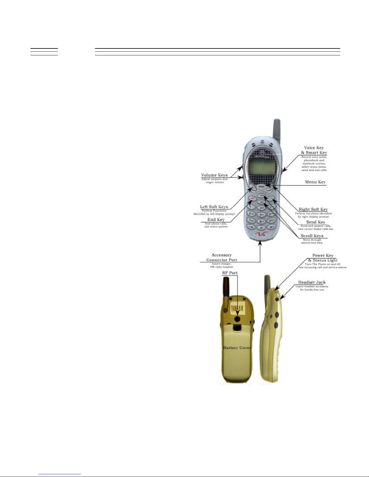
General:
Tarpon V. 120C Product Description
V.120C also known as Tarpon is based on CDMA platform
2000 reference architecture. This is a Dual Band Tri Mode
phone- 1900Mhz CDMA /800 Mhz CDMA/ 800Mhz AMPS.
Innovative contoured design combine style and comfort in a
small, sleek phone available in two colors,
Arctic silver and Navy Blue which can be personalized through
interchangeable phone Wrap which are available in different
colors and materials.
Product Description
Large 96 X 64 Graphic LCD Display offering 4 lines of text, 1
line of icons and 1 line of prompts, improved usability with the
new synergy user interface.
WAP 1.1 enabled micro browser, voice recognition driven
dialing and short cuts, 32 alert tones,vibraCalldiscreet alert,
Mobile originated and Mobile terminated SMS messaging,
Fixed stub antenna.
A complete line of accessories, including FM stereo, Phone
wrap covers, travel charger, headsets, vehicle power adapter,
swivel belt clip and data connectivity kit.
19 keys on the keypad for synergy support. Volume keys and
smart key on the sides. Integrated headset jack on the top above
which is the power button and service indicator LED.
Accessory connector: 17 pin CE bus connector,
access to USB, RS232, power, ground, analog and digital
audio, FM stereo headset.
Batteries: Lithium ion (600 mAh -6mm and 1100 mAh - 8mm)
© 2001 Motorola, Inc. 4

V.120c
Product Description
V.120c LOGIC CIRCUIT
The main chip sets of Platform 2000 reference architecture
products consists of WALLY and CCAP IC. The memory
chips are the FLASH and the RAM.The WALLY includes the
functionality of CPU + DSP + CSP + CIA. The WALLY is M Core product (Motorola Proprietary) 32 bits. The CCAP IC
works in Buck mode and provides the power management
function of the phone. It also does the audio amplification and
routing. It controls the 32Khz crystal, it interfaces with
WALLY on 8 bit Parallel Bus. The communication to the
accessories through the CSS bus connector is done through the
CCAP IC. The audio through the external connector is digital.
All audio interface is through CCAP IC - Alert, Phone Speaker,
headset speaker & Microphone, External Speaker &
Microphone, and Phone Microphone
The Wally IC integrates the functionality of Casper IC (which
contains the MCU,
RIB, the CSP and the DSP) and CIA
Key features of the WALLY IC:
- M-Core integer processor, 32 bit RISC architecture
10-bit AOC -loop control ADC and DAC
(DSP peripheral)
A UART with auto baud detection
Universal serial bus (USB) interface module
Serial Audio Port interface
Key features of the CCAP IC:
CCAP IC uses Buck converter mode with no 5V supply
- 8 bit parallel interface from Wally
- Buck and Boost converters
- 8-Linear voltage regulators
- 2-Hi end linear regulators w/ common
reference (PA Drain regulators)
- External B+ clamp regulator
- 3 Microphone Amplifiers
- Differential audio interfaces to and from
Wally
- Audio Amps,Multiplexers and Speaker &
Alert Drivers
- 56600 NDE-UL DSP Core running at up to 70 Mhz @ 1.8V
- MCU -DSP interface
- CDMA signal processor (CSP3) ASIC
- 16 bit external memory interface for the MCU
- 8 bit parallel interface for CCAP
- 32-Input Interrupt Controller for the MCU
-Internal MCU ROM and RAM
- Special modules for CDMA mode
(all are MCU peripherals):
- Dual 9.8304 M samples/sec 4-bit ADCs
(RX I/Q with Receive AGC)
- Dual 4.9152 M samples/sec 9-bit DACs
- 13-bit linear CODEC
- 1-8bit, 2-10bit, 1-12bit measurement DAC
- 8-bit measurement ADC with 6 multiplexed inputs
© 2001 Motorola, Inc. 5
- Headset and Send/End key detection
- Battery charger
- 6 input 8 bit ADC
- Real time clock (RTC) with coin cell
backup supply and coin cell charger
- Timer circuits
- CE bus interface
- Vibrator and Backlight regulator inside the
CCAP IC
The external memory consists of 32 Mega bit 1.8V FLASH and
4 Mega bit 1.8V SRAM
The butt plug is a 17 pin CE bus connector , which supports
the USB and RS232 Serial communications. CE bus runs at
1.8V.
V.120c Supports a complete line of accessories including FM
stereo. FM Radio headset (SYN8609) plugs into the CE bus
connector.
V.120c will not support the 3WB or PST mode of
communications.
Keypad connector is a 14 pin data no mating

V.120c
Product Description
connector-keypad, compression type
32 Khz crystal controlled by CCAP IC for RTC and slotted
mode operation.
The charging circuit consists of Fast charger which is similar to
StarTac , V.120c phones will also support Mid Rate charger
The flex connector interfaces the main board with the Display,
Speaker and the RTC Battery in the flip.
The accessory antenna port is present on the back side of the
phone near the antenna.
All the logic parts and IC’s are placed on one side and all RF
parts and IC’s are placed on another side of the PCB
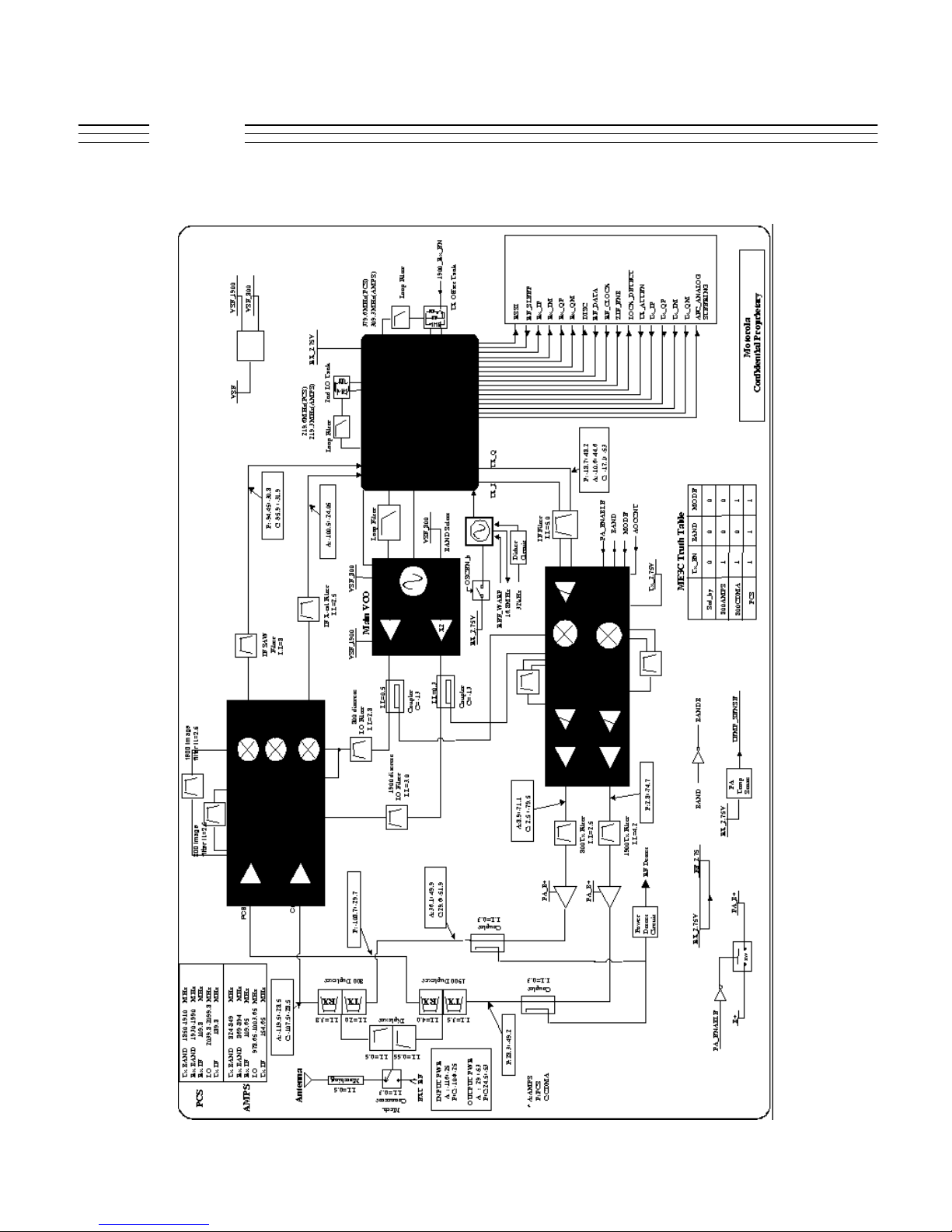
V.120c RF CIRCUIT
The RF circuit is somewhat similar to Dual band Caliber/Shark
product, the V.120c phone contains FE IC (the front end IC)
ZIF/SYN IC controls the Main VCO ,the second LO and the
TX offset VCO (in analog mode).
V.120c uses the single VCO module for main
LO (one for the 800 mhz band and another for PCS band) The
output is split into RX_LO and TX_LO
for both the bands.
V.120c uses the ME3 IC - the mixer exciter IC
The ME3 IC allows to control the RF output power. The ME3
IC requires two LO’s, one for PCS, and the other for the 800
Mhz band.
The IF pins (input to the ME3 IC) are the same for any band.
The control signal (TXAtt) at the AGC pins control the gain of
the ME3 IC.
There is an external interstage RF filter between the mixer and
exciter.
The receiver contains two complete receiver paths : 800 Mhz
path that is used by 800 Mhz analog and 800 Mhz CDMA
signals, and a PCS band(1900Mhz) path for PCS signal. The
two paths have different RF, LO and IF frequencies.
The switching of the antenna and accessory antenna port is
mechanical, normally close circuit with antenna connector, but
when accessory RF cable is inserted in the accessory port the
switch opens the circuit with antenna and closes the circuit with
the accessory port.
For Frequencies and channel numbers look at the table in this
manual
The FE IC contains the LNA’s , interstage filtering and Mixers,
the switching and gain of the LNA’s is controlled by the
control signals
ZIF/SYN IC extracts the broadband signal from the IF ,
demodulate the analog signal and sends it to the audio logic
side for further processing.
Balun is a component external to ME3 IC and is not a discreet
part as in V.60c
From the mixer the outputs take two different paths one for TX
PCS band and another for TX 800Mhz band.
ME3 IC has 50dBM attenuator control (input IF level= 23dBM , max output TX level= 25dBM)
At the output of ME3 IC band filter are used , in the PCS path
two split band filters are used. V.120c uses celeritek PA HBT
and not MOSFET as in V.60c.
Two stage PA in 800 Mhz band and three stage PA in PCS
band .
In V.120c PA adjustable bias only Drain therefore the output
power can be controlled by PA_B+ DAC besides ME3 IC
(through Tx_Attn). PA gate Bias is not adjustable but fixed and
regulated at 2.95v.
© 2001 Motorola, Inc. 6

V.120c
Theory of Operation
I. AMPS
RECEIVER
RECEIVER CIRCUITRY
Theory of Operation
The phone receives the RF signal from the Antenna or the
RF test port, the received RF signal is routed through the
Diplexer - FL11 to mono block duplex SAW filter –
FL12. The RF signal is then routed to the Front End
IC(FE IC) – U100 , which contains LNA which provides
a 10 -12 dB gain to the received RF signal, and U100
provides inter stage filtering and it contains Mixer which
down converts the frequency of the signal to IF which is
109.65Mhz.
The local oscillator signal which is input to the FEIC is
978 – 1004Mhz. The VCO module U680 is controlled by
the ZIF/SYN IC – U932.
The mixer output IF signal 109.65Mhz is routed through
IF filter - FL201 into the ZIF/SYN IC U932 for mixing
with the second LO ,filtering and demodulation.
RECEIVER AUDIO
DISC - signal an AMPS discriminator audio which is the
output of FM demodulator in U932 is produced by mixing
the IF signal with the second LO (which is controlled by
U932) and then filtered. The audio on DISC line goes to
WALLY IC -U1100 to be digitized. All receive audio
filtering and gain control is performed in the digital
domain within the WALLY which contains DSP, the
processed RX audio is converted back to analog and
routed to CCAP IC – U2000 on signals AUDIO_P and
AUDIO_M.
The CCAP - U2000 amplifies and route the audio
signal(receive audio) to the speaker (phone speaker,
boom speaker or external speaker). The alert tone
originates in WALLY IC and follows the same path as
receive audio except from CCAP it is routed to the
alert.
TRANSMITTER
TRANSMITTER AUDIO
Audio from the Microphone (internal, boom or
external) is routed through and amplified by CCAP –
U2000 and then travel to the WALLY IC – U1100 on
MIC1 and MICREF lines which is digitized by the
CODEC inside the WALLY and the DSP present in
WALLY performs the compression, pre-emphasis,
limiting and band pass filtering function in the digital
domain. All Amps signaling (SAT, ST, DTMF) is
also generated in the digital domain by the DSP inside
the WALLY. The digitized amps TX audio signal is
converted back to analog inside the WALLY and
© 2001 Motorola, Inc. 7

V.120c
Theory of Operation
sent on FM line to the 154.8MhzTx offset VCO to
modulate the transmitter frequency.
TRANSMITTER CIRCUITRY
The FM signal from WALLY modulates the Tx
offset VCO signal which is external but controlled
by ZIF/SYN – U932. The Tx IF modulated signal
154.8Mhz is input to the ME3 IC – U600 where it
get mixed with the 979 – 1004 Mhz local oscillator
signal. The Tx signal then passes through the band
pass filter FL605 into the Power Amplifier (PA) –
U430 where it is amplified and the output passes
through the isolator U550 and then through TX
band pass mono block duplex SAW filter FL12 and
through diplexer FL11 to the antenna or RF test
port.
II. CDMA CELLULAR (800Mhz) MODE OF
OPERATION
RECEIVER
RECEIVER CIRCUITRY
RECEIVER AUDIO
Four outputs from U932 – RXIP, RXIM,
RXQP, RXQM carries the base band signal of
the receive digital call to the WALLY, the
received QPSK data is gain controlled and
converted to digital, the 1.2288 Mb/sec Rx data
stream is then decoded by the CSP inside the
WALLY to produce a signal containing only the
desired data. The digital speech data is further
decoded by the CELP vocodera part of DSP
within WALLY and then converted back into
analog receive audio and routed to CCAP IC –
U2000 on signals AUDIO_P and AUDIO_M.
The CCAP - U2000 amplifies and route the
audio signal (receive audio) to the speaker
(phone speaker, boom speaker or external
speaker). The alert tone originates in WALLY
IC and follows the same path as receive audio
except from CCAP it is routed to the alert.
TRANSMITTER
TRANSMITTER AUDIO
The phone receives the RF signal from the Antenna
or the RF test port, the received RF signal is routed
through the Diplexer - FL11 to mono block duplex
filter – FL12. The RF signal is then routed to the
Front End IC(FE IC) – U100 , which contains LNA
which provides three stage gain to the received RF
signal based on its strength, and U100 provides inter
stage filtering and it contains Mixer which down
converts the frequency of the signal to IF which is
109.8Mhz.
The FE IC is controlled by WALLY through the
following signals: FEIC_G1, FEIC_G2, and MODE.
The local oscillator signal which is input to the
FEIC is 978 – 1004Mhz. The VCO module U680 is
controlled by the ZIF/SYN IC – U932.
The mixer output IF signal 109.8Mhz is routed
through IF filter- FL200 into the ZIF/SYN IC U932
for mixing with the second LO ,filtering and
demodulation.
© 2001 Motorola, Inc. 8
Audio from the Microphone (internal, boom or
external) is routed through and amplified by
CCAP – U2000 and then travel to the WALLY
IC – U1100 on MIC1 and MICREF lines which
is digitized by the CODEC inside the WALLY
and the DSP present in WALLY processes by
CELP variable rate vocoderand then processed
by the modem (CSP) within the WALLY which
produces the 1.2288Mb/sec CDMA data
stream. This stream is then converted to analog
signals and send to ZIFSYN IC on four lines
TXIP, TXIM, TXQP, TXQM. This modulates
on the TX IF (QPSK modulation) 154.8Mhz
TX offset VCO.

V.120c
Theory of Operation
from WALLY modulates the Txoffset VCO signal
which is external but controlled by ZIF/SYN –
U932. The Tx IF modulated signal 154.8Mhz is
input to the ME3 IC – U600 where it get mixed
with the 979 – 1004 Mhz local oscillator signal.
The Tx signal then passes through the band pass
filter FL605 into the Power Amplifier (PA) – U430
where it is amplified and the output passes through
TX band pass mono block duplex filter FL12 and
through diplexer FL11 to the antenna or RF test
port.
III. CDMA PCS (1900Mhz) MODE OF
OPERATION
RECEIVER
RECEIVER CIRCUITRY
The phone receives the RF signal from the Antenna
or the RF test port, the received RF signal is routed
through the Diplexer - FL11 to mono block duplex
ceramic filter – FL10. The RF signal is then routed
to the Front End IC(FE IC) – U100 , which contains
LNA which provides three stage gain to the
received RF signal based on its strength, and U100
provides inter stage filtering and it contains Mixer
which down converts the frequency of the signal to
IF which is 109.8Mhz.
The FE IC is controlled by WALLY through the
following signals: FEIC_G1, FEIC_G2, and
MODE.
The local oscillator signal RX_LO_PCS is 20392100Mhz. The VCO module U680 is controlled by
the ZIF/SYN IC – U932.
The mixer output IF signal 109.8Mhz is routed
through IF filter- FL200 into the ZIF/SYN IC U932
for mixing with the second LO ,filtering and
demodulation.
RECEIVER AUDIO
Four outputs from U932 – RXIP, RXIM,
RXQP, RXQM carries the base band signal
of the receive digital call to the WALLY, the
received QPSK data is gain controlled and
converted to digital, the 1.2288 Mb/sec Rx
data stream is then decoded by the CSP
inside the WALLY to produce a signal
containing only the desired data. The digital
speech data is further decoded by the CELP
vocodera part of DSP within WALLY and
then converted back into analog receive
audio and routed to CCAP IC – U2000 on
signals AUDIO_P and AUDIO_M.
The CCAP - U2000 amplifies and route the
audio signal (receive audio) to the speaker
(phone speaker, boom speaker or external
speaker). The alert tone originates in
WALLY IC and follows the same path as
receive audio except from CCAP it is routed
to the alert.
TRANSMITTER
TRANSMITTER AUDIO
Audio from the Microphone (internal, boom
or external) is routed through and amplified
by CCAP – U2000 and then travel to the
WALLY IC – U1100 on MIC1 and MICREF
lines which is digitized by the CODEC
inside the WALLY and the DSP present in
WALLY processes by CELP variable rate
vocoderand then processed by the modem
(CSP) within the WALLY which produces
the 1.2288Mb/sec CDMA data stream. This
stream is then converted to analog signals
and send to ZIFSYN IC on four lines TXIP,
TXIM, TXQP, TXQM. This modulates on
the TX IF (QPSK modulation) 189.8Mhz
TX offset VCO.
TRANSMITTER CIRCUITRY
The four signals TXIP, TXIM, TXQP,
TXQM
© 2001 Motorola, Inc. 9

V.120c
TRANSMITTER CIRCUITRY
Theory of Operation
The four signals TXIP, TXIM, TXQP, TXQM from
WALLY modulates the Txoffset VCO signal which is
external but controlled by ZIF/SYN – U932. The Tx IF
modulated signal 189.8Mhz is input to the ME3 IC –
U600 where it get mixed with the 2039-2100 Mhz local
oscillator signal. The Tx signal then passes through the
filter FL601 into the Power Amplifier (PA) – U900
where it is amplified and the output passes through TX
band pass mono block duplex filter FL10 and through
diplexer FL11 to the antenna or RF test port.
FREQUENCY SYNTHESIZER CIRCUITRY
The phone contains three PLL frequency synthesizers
controlled by U932.
1. The main VCO : there is only one VCO modules which controls the tunable 979 – 1004Mhz main local
oscillator – and is ON during Cellular or 800Mhz mode.
and also controls the tunable 2039-2100Mhz main local
oscillator, which is ON during PCS or 1900Mhz mode.
2. The Tx offset VCO: there are two modes and two
frequency at which this oscillator which is internal to
U932 works, but the tank circuit is external. There are
two tank circuits one for Cellular mode (800Mhz)
which will set 309.6Mhz frequency for the oscillator to
oscillate on. Another tank circuit for PCS mode
(1900Mhz) which will set 379.6Mhz frequency for the
oscillator to oscillate on. The Tx offset frequency is
divided by 2 before being fed into the mixer for
modulation.
All the synthesizers obtain their reference
frequency from the 16.8Mhz reference
oscillator.
TRANSMIT POWER CONTROL
CIRCUITRY
The transmit signal power (the output RF power)
is controlled by the three control signals
ZIF_VCA and ME_VCA from WALLY IC and
PA_VCC from CCAP IC. The output power is
controlled at three places, ZIFSYN – U932 which
has a gain control of max 40dB and ME3 ICU600 which has a total gain of max 36dB and PA
has a gain of max 27-32dB.
In Amps mode the power range is +8dBM to
+28dBM. In CDMA mode the RF power range is
from –50dBM to +23dBM.
In CDMA mode the power control operates in
two mode: Open loop and Close loop. In open
loop mode (at the beginning of registering –
access probe) the power level is proportional to
the received signal level, in close loop mode the
power level is controlled by the CDMA cell based
on the received signal strength at the cell site.
3. The second LO: the second local oscillator also
operates in two modes with two different frequencies:
For AMPS mode the frequency is 219.3Mhz and for
CDMA mode at cellular or 800Mhz band and PCS or
1900Mhz band the frequency is 219.8Mhz. The tank
circuit is external to the U932. The frequency is divided
by 2 before being fed into the mixer.
© 2001 Motorola, Inc. 10
V.120c
Theory of Operation
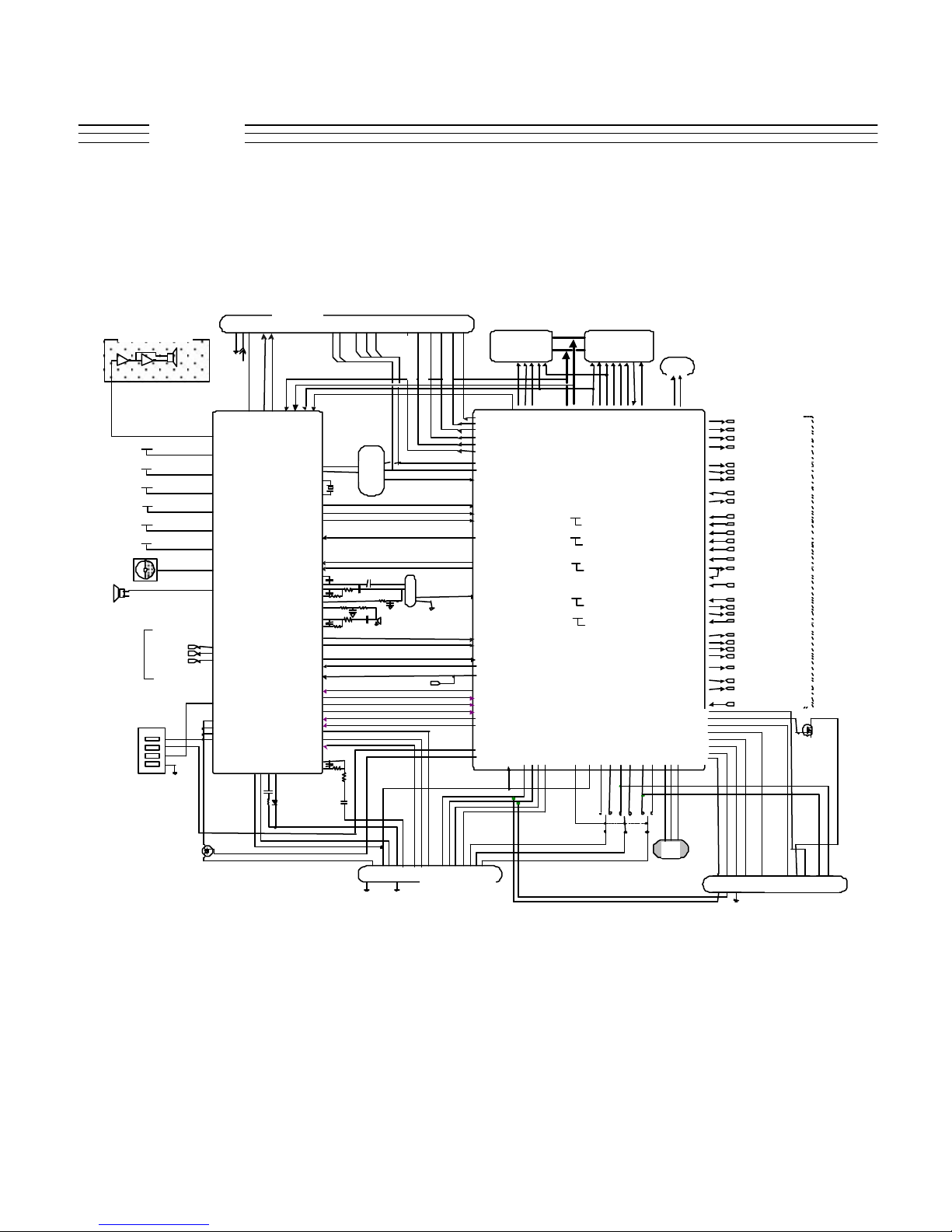
AUDIO LOGIC BLOCK DIAGRAM
PANTHER OPTION ONLY
Digital_1.8V
Analog_1.8V
Memory_Vcc
Logic_2.75v
RX_2.75v
TX_2.75v
B+
Alert
PAH_B+
PAL_B+
32KHZ
To RF
Section
4
3
2
BATTERY
CONTACTS
1
BATT_GND
Speaker
Phone
AUDFB
V1A
V1B
V2
V3
V5
V6
V9(VIBOUT)
A2OUT
PAH_B+
PAL_B+
32KHZ
MAINTEMP
MAINBATT
VIN9
VIN8
B+
LOGIC_GND
LOGIC_2.75v
RTCBATT
FEEDBACK
Flex to Flip
Display Driver Connector J3000
KBR1
KBR2
A_Db
R_Wb
DATA[7:0]
CCAPCEb
SPKROUTP
SPKROUTM
V8(Led_Backlgt)
ON1b
XTAL1
32 KHz
XTAL2
32KHZ CKIL
RESETb
INTb
WDI
CCAP & Ckts
AUDPIN
AUDMIN
A3IN
A3OUT
MIC2MIN
MIC2OUT
VMIC2
VMIC1
MIC1MIN
MIC1OUT
MIC4OUT
MIC4REF
PAH_D_PHASE
V10EN
USBOEb
USBVMOUT
USBVPOUT
USBRXD
USBVMIN
USBVPIN
USBP
USBM
USBPWR
MIC3OUT
MIC3MIN
A4OUT
RAWEXTB+
ON2b
CDMA Brassboard Baseband
KBC5
KBC6
KBC1
J2000
Conn.
Keypad
Int.
Mic.
PA_ENABLE
Ser_LCD_A0
Ser_LCD_MOSI
RESET_OUT_b
HEADSET
LCD_CS
LCD_CS1
Ser_LCD_CLK
LCD_CS
LCDCS1
Ser_LCD_A0
Ser_LCD_MOSI
RESET_OUT_b
KEY_COL[:4]
KEY_ROW[0:5]
INT0 (FLIP_OPEN_B)
RESET_IN_B
INT4_B
STO
AUDIOOUTP
AUDIOOUTM
INT1 (HEADSET_DET)
MIC1
MIC_REF
THERM1
RXATTENV10REF
PAENABLE_LO
USB_OE
RXDP
USB_VP
RTSP
USB_VMO
TXDP
GPIO8
GPIO6
Ser_LCD_CLK
CS2_B
MCI0
UB
EB0_b
DCDPB
LB
EB1_b
EN_CS
DTRPB
EN_OE
EN_WE
CS1_B
WALLY
OPTION2
OPTION1(INT6)
EN_WE
R_WB
DATA[15:0]
ADDR[21:0]
V1a (1.8 V)
QVCC(1-5)
V1b (1.8 V)
ANOLGVDD(1-3)
SDVDD(1-2)
V2 (1.8 - 2.75 V)
AVDD(1-2)
CVDD
DVDD
V5 (2.75)
EALOGVDD(1-2)
V3 (2.75 V)
QVCCH(1-4),
GVDD(1-3),
HVDD(1-2),
KVDD, UVDD
KEY_ROW3
RTSB_ALT
FLASHRAM
BAA
EN_OE
EN_CE
OEB
CS0B
GPIO10/BAA_B
CTSB_0WIRE
CTSB_ALT
RESET
ADV
BCLK
WAIT
BOOTMOD
CS3_B/BCLK
RESET_OUT_B
GPIO11/WAIT_B
RXDP_ALT
TXDP_ALT
RIPB
Motorola Cellular Subscriber
Confidential Proprietary
Status
LED
FEIC_G1GPIO0
GPIO1
GPIO2
GPIO3
RXIM
RXIP
RXQM
RXQP
DISC
GPIO7
MCI1
RSSI
AFC
CKIH
TXIM
TXQP
TXQM
MISO
SRDA
STDA
SCKA
SC2A
FM
FEIC_G2
BAND
MODE
RFCLK
RFDATA
ZIF_ENB
LOCK_DETECTGP109
RF_SLEEP
RXIM
RXIP
RXQM
RXQP
DISC
AFC_ANALOGSTEERING
ZIF_VCA
RSSI
RF_DETRFDETECT
OSCEN_b
16.8Mhz
TXIPTXIP
TXIM
TXQP
TXQM
FM
ME_VCAAOCCNT
PA_BIAS
TEMP_SENSE
INT0(SM_DET)
DSRPB
RXDS_ALT
GPIO4
LED_DR1
LED_DR0
RFCLK
RFDATA
SPICS3
RXCTRLB
TXATTEN
OSCENB
PA_BIAS
THERM0
SPICS0
SPICS1
TXDS_ALT
To RF Section
REF_WARP
BATT_SERIAL_DATA
SW_B+_EN
Motorola Cellular Subscriber
Confidential Proprietary
AUDIO_GND
ESD protection not shown
2 3 467 95
15
16
1
17
BATT_GND
11
10812
14
13
CSS Bus Connector J1000
DATALOG
_CNTRL_b
NC
NO
IrDA
XCVR
For future use on
Panther
Panther Option Only
© 2001 Motorola, Inc. 11
ESD protection not shown
10 11 13 12
869
BATT_GND
16
15 7 14
CE Module Bus Connector
12
V.120c
Theory of Operation
RF SIDE BLOCK DIAGRAM
© 2001 Motorola, Inc. 12

V.120c
Disassembly
Disassembly
Introduction
Care must be taken during the
disassembly and reassembly of the unit
in order to avoid damaging or stressing
the housing and internal components.
Ensure that a properly grounded high
impedance conductive wrist strap is
used while
performing these procedures on
electronic units.
Recommended Tools
The following tools are recommended
for use during the disassembly and
reassembly of the phone.
- Anti-Static Mat 6680387A95
- Ground Cord 6680334B36
- Wrist Band 4280385A59
_ Plastic Prying Tool SLN7223A
CAUTION
Many of the integrated circuit devices
used in this equipment are vulnerable to
damage from static charges. An antistatic wrist band, connected to an antistatic (conductive) work surface, must be
worn during all phases of disassembly,
repair, and reassembly.
Disassembly Procedure
Refer to the disassembly instructions and
photo sequence on the following pages.
Assembly Procedure
Once the unit is disassembled and the
repair
is carried out it then becomes obvious
that to
_ Rear Housing Removal Tool
_ Dental Pick
_ Tweezers
- T6 Torque Screw Driver
assemble the unit, the procedure is the
reverse of that previously completed for
disassembly.
© 2001 Motorola, Inc. 13
V.120c
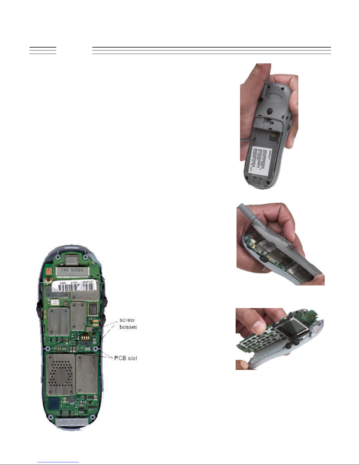
Rear Housing Removal:
Using a generic screw driver unscrew all the 6
screws. Gently remove the Rear Housing as
shown.
Disassembly
Board Removal:
The six screw bosses hold the board in place.
Remove the board as shown.
Board Removal
© 2001 Motorola, Inc. 14
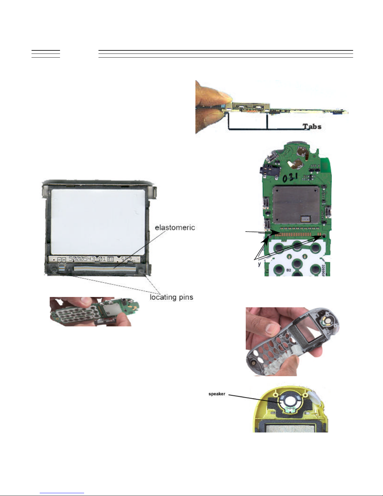
V.120c
Display Removal:
The electrometric on the display makes contact
with the power contacts on the PCB. There are
two locating pins on the display are aligned and
the four holding tabs are grabbing the board.
Make sure you release the tabs and gently lift the
display. Once you free the tabs on one side, the
other side comes off easily.
Disassembly
Keypad Removal:
Remove the keypad from the front housing as
shown.
Speaker Removal:
Pads On
The PCB
Holes For
Display
Locating
Pins
There is a adhesive backing to the speaker,
hence make sure you pry the speaker open by
the help of a bezel stick.
© 2001 Motorola, Inc. 15
V.120c
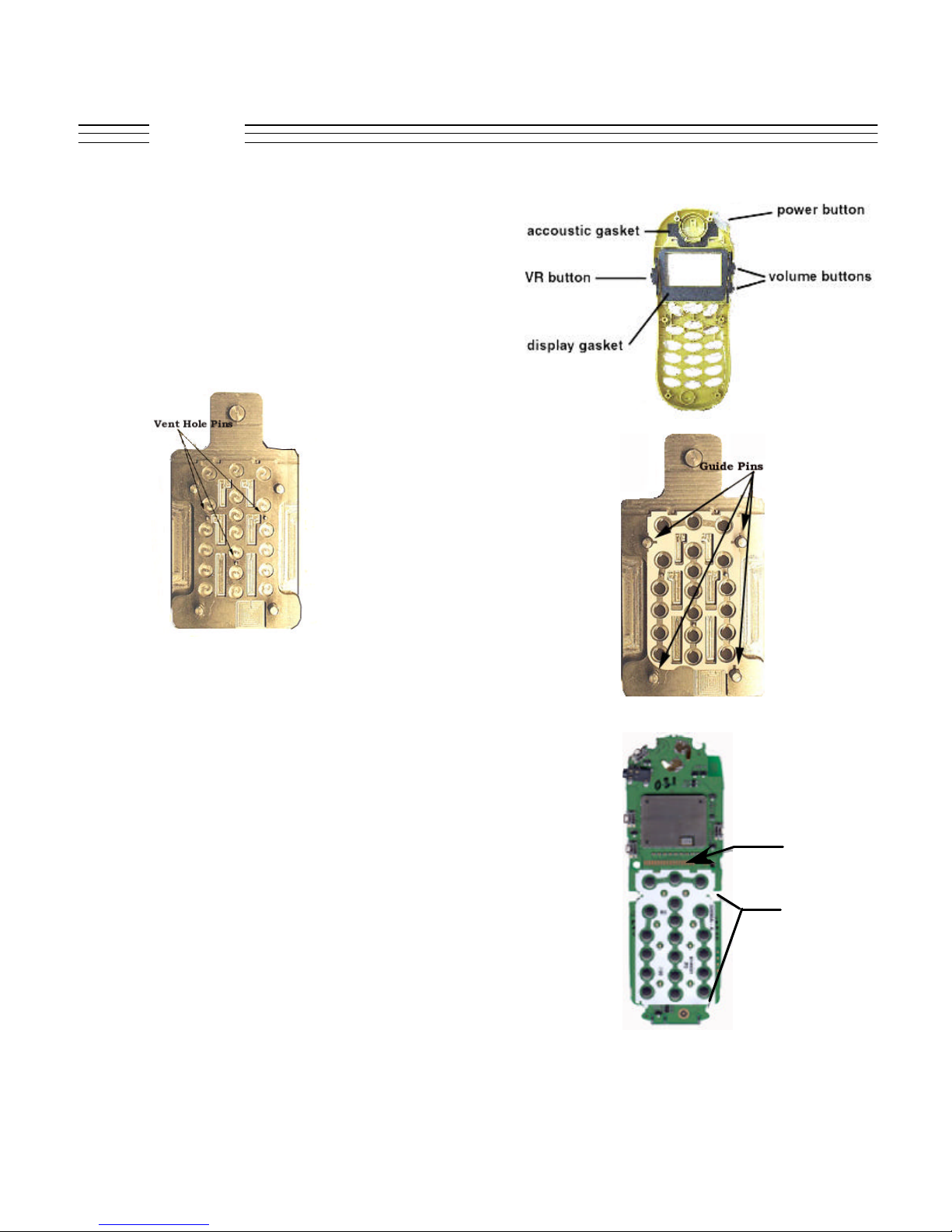
Acoustic Gasket, Power Button, VR Button<
Volume Buttons and Display Gasket Button
Removal:
All of the above accessories are placed in their
respective places and are easily removable.
Disassembly
Mylar installing tool
Mylar located in Between The Pins
Contacts
Cutouts
Mylar Place On The Board
© 2001 Motorola, Inc. 16
V.120c
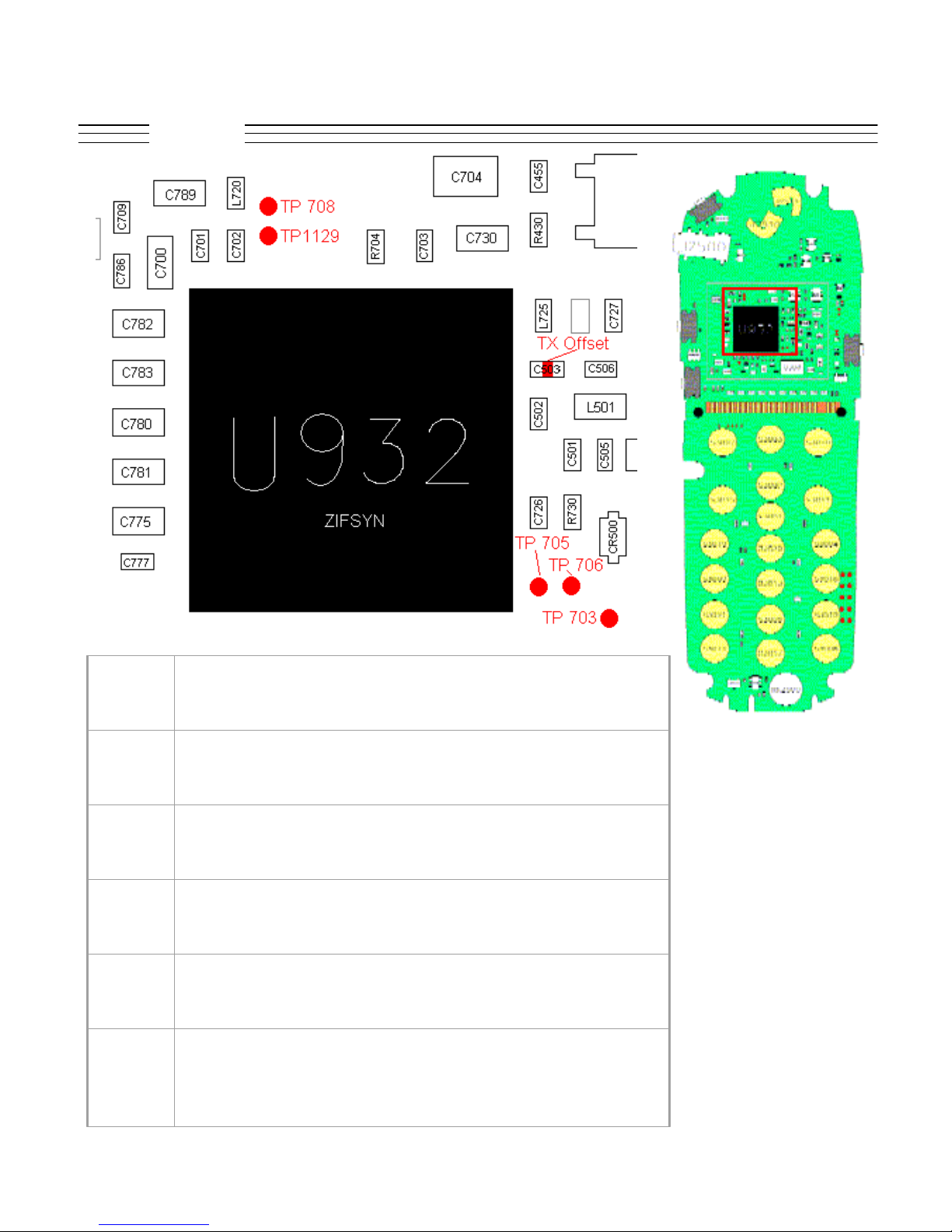
Troubleshooting
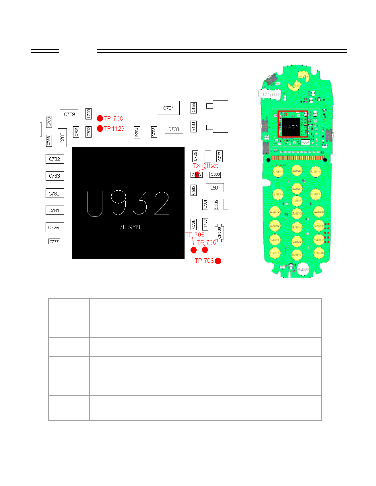
C503 Offset VCO, sniff to avoid loading, cell=309.6, PCS=379.6
TP703 TXIP
TP705 TXQM
TP706 TXQP
TP708 LOCKDETECT
TP1129 AFC_ANALOGSTEERING
© 2001 Motorola, Inc. 17
V.120c
Troubleshooting
C503 Offset VCO, sniff to avoid loading, cell=309.6, PCS=379.6
TP703 TXIP
TP705 TXQM
TP706 TXQP
TP708 LOCKDETECT
TP1129 AFC_ANALOGSTEERING
© 2001 Motorola, Inc. 18
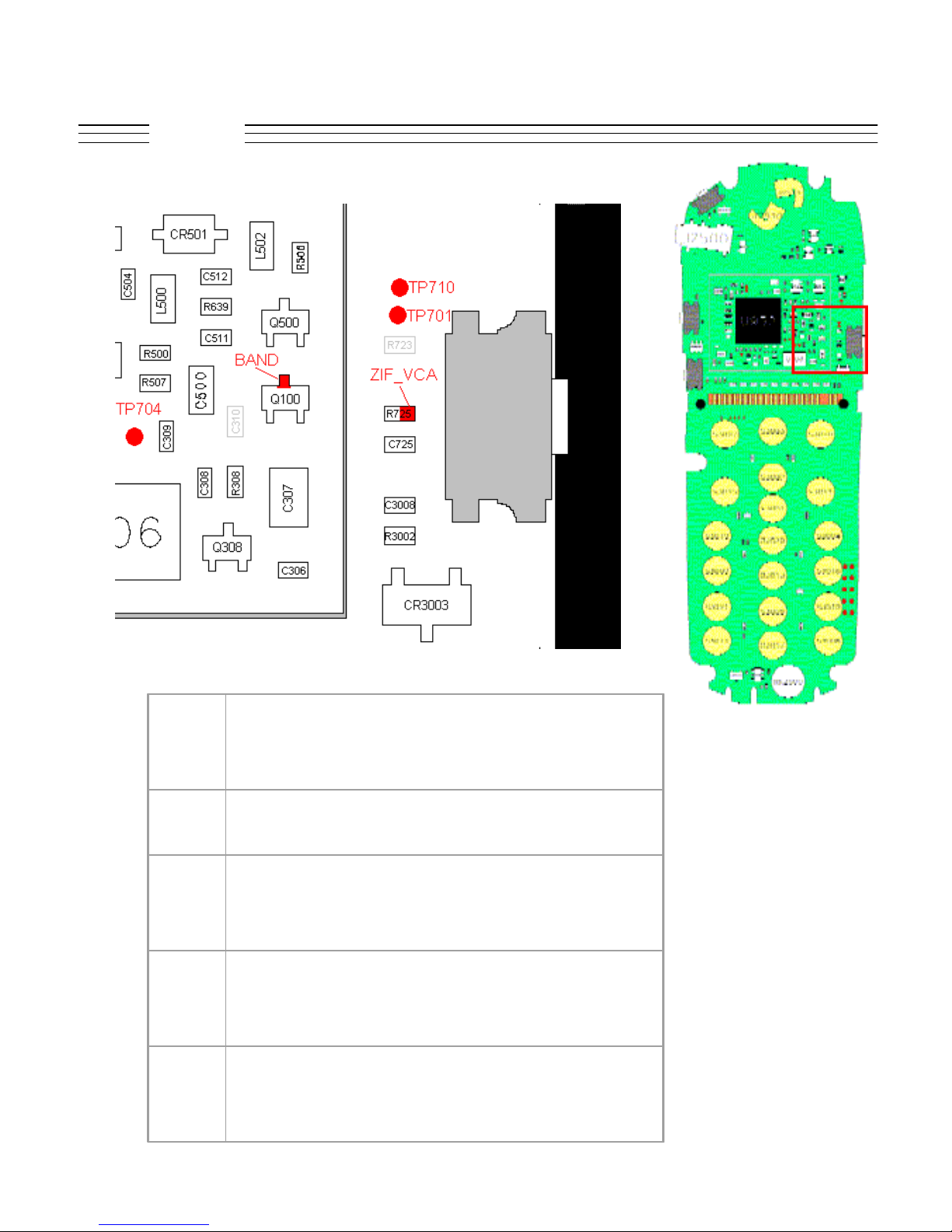
V.120c
Troubleshooting
Q100 BAND
R725 ZIF_VCA (analog signal)
TP701 RSSI receiver signal strength (analog signal)
TP704 TXIM
TP710 RF_CLOCK
© 2001 Motorola, Inc. 19
V.120c
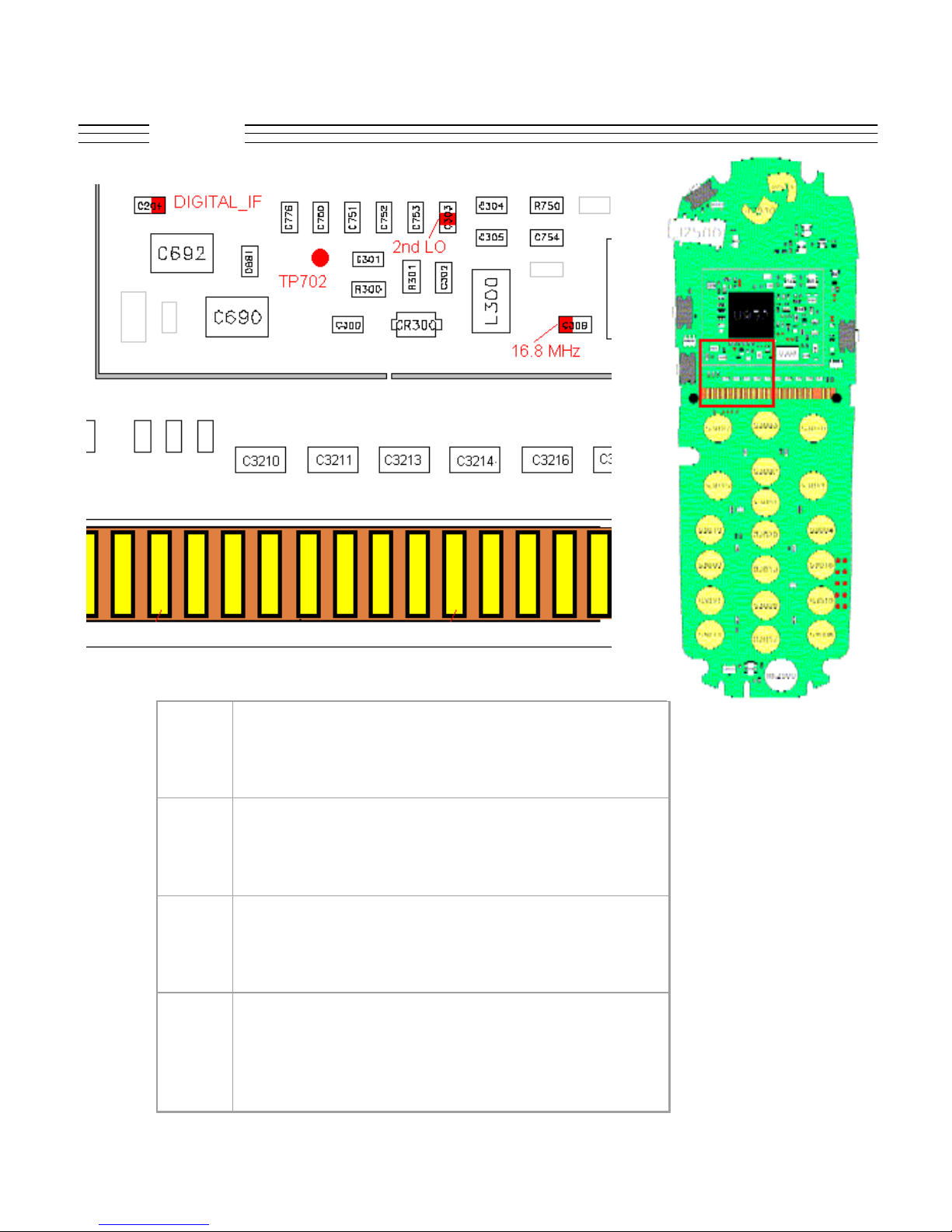
Troubleshooting
C204 RX IF to ZIFSYN, level is approx equal to input level
C303 2nd LO, 219 MHz
C308 16.8 MHz oscillator output
TP702 MTESTP
© 2001 Motorola, Inc. 20
V.120c
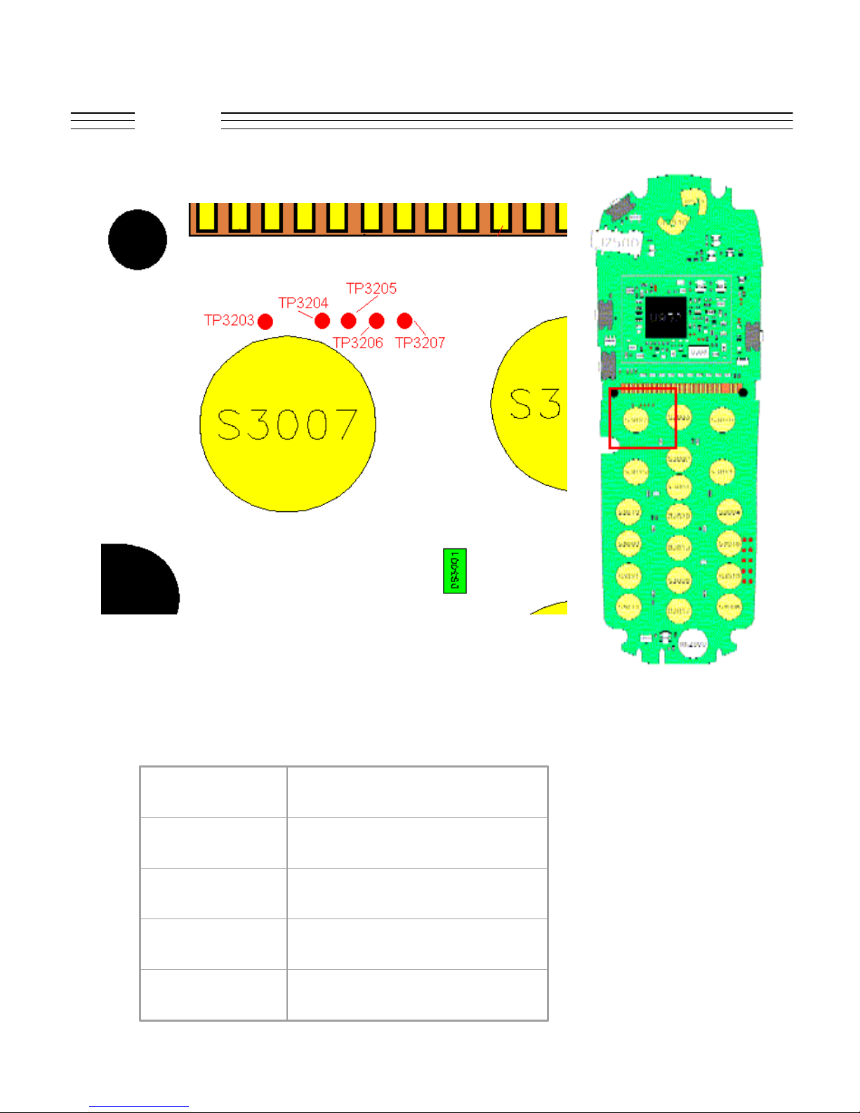
Troubleshooting
TP3203 LCD_CS
TP3204 RESET_OUTb
TP3205 LCD_A0
TP3206 LCD_CLK
TP3207 LCD_MOSI
© 2001 Motorola, Inc. 21
V.120c
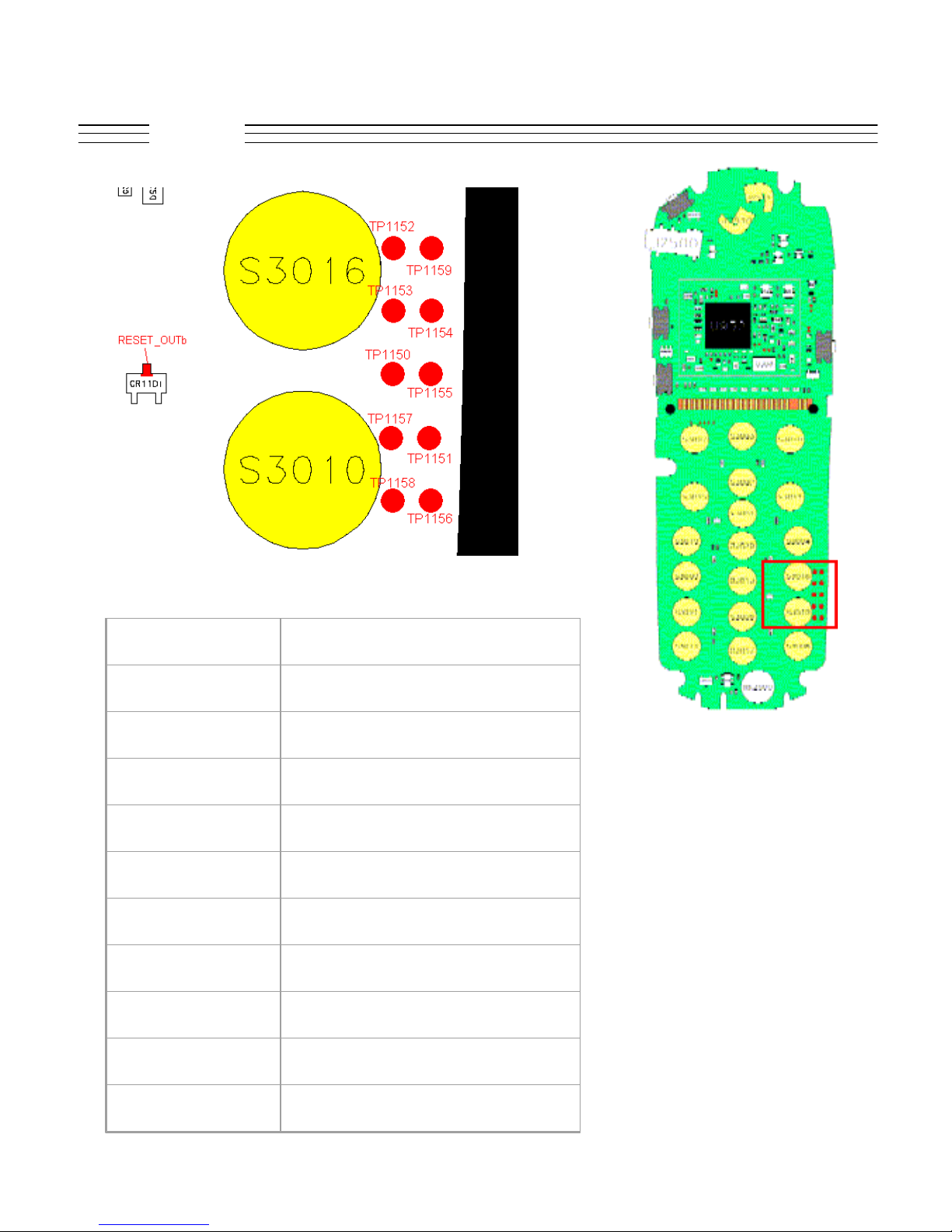
Troubleshooting
CR1101 RESET_OUTb
TP1150 JTAG interface
TP1151 JTAG interface
TP1152 JTAG interface
TP1153 JTAG interface
TP1154 JTAG interface
TP1155 JTAG interface
TP1156 JTAG interface
TP1157 JTAG interface
TP1158 JTAG interface
TP1159 JTAG interface
© 2001 Motorola, Inc. 22
V.120c
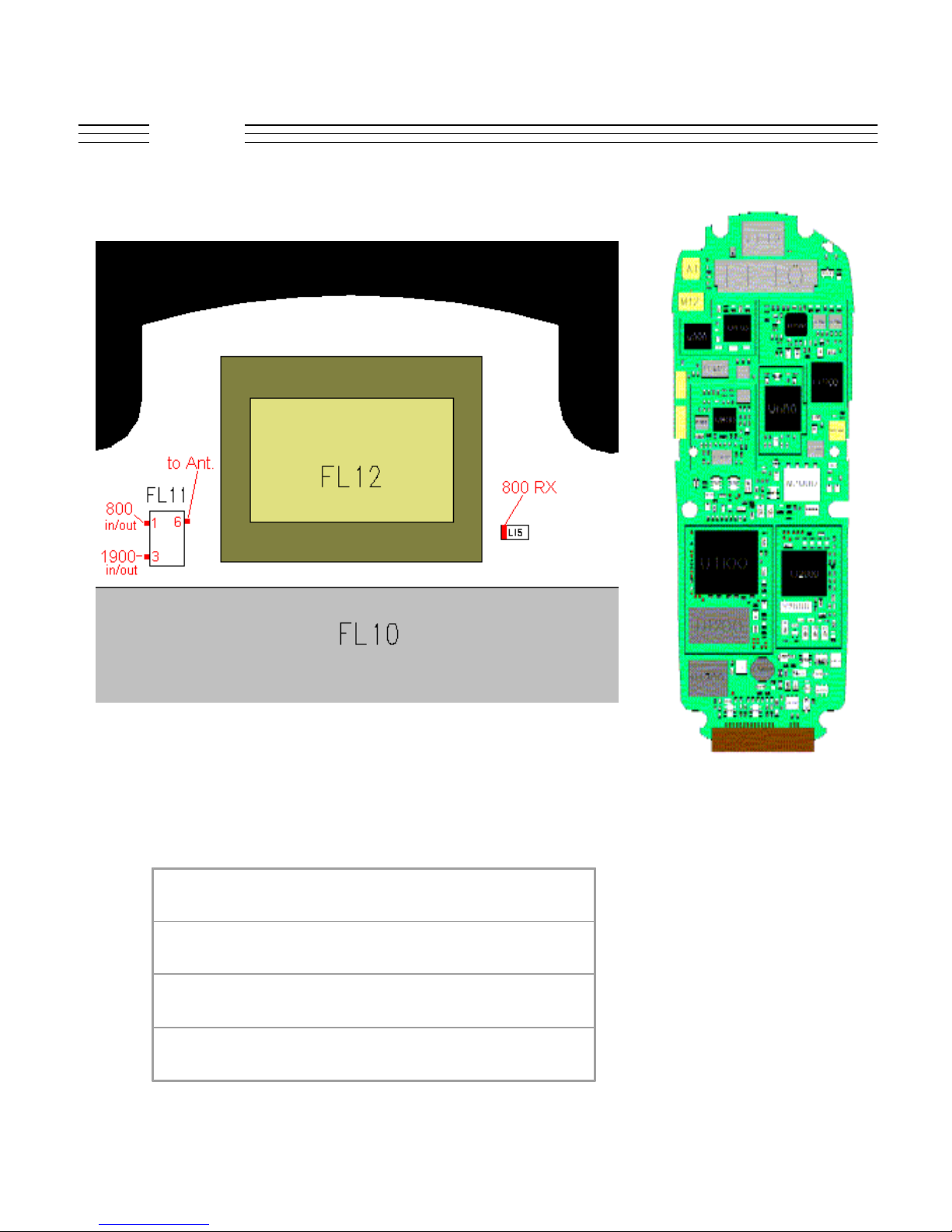
Troubleshooting
FL11 - 1
FL11 - 3
FL11 - 6
L15
© 2001 Motorola, Inc. 23
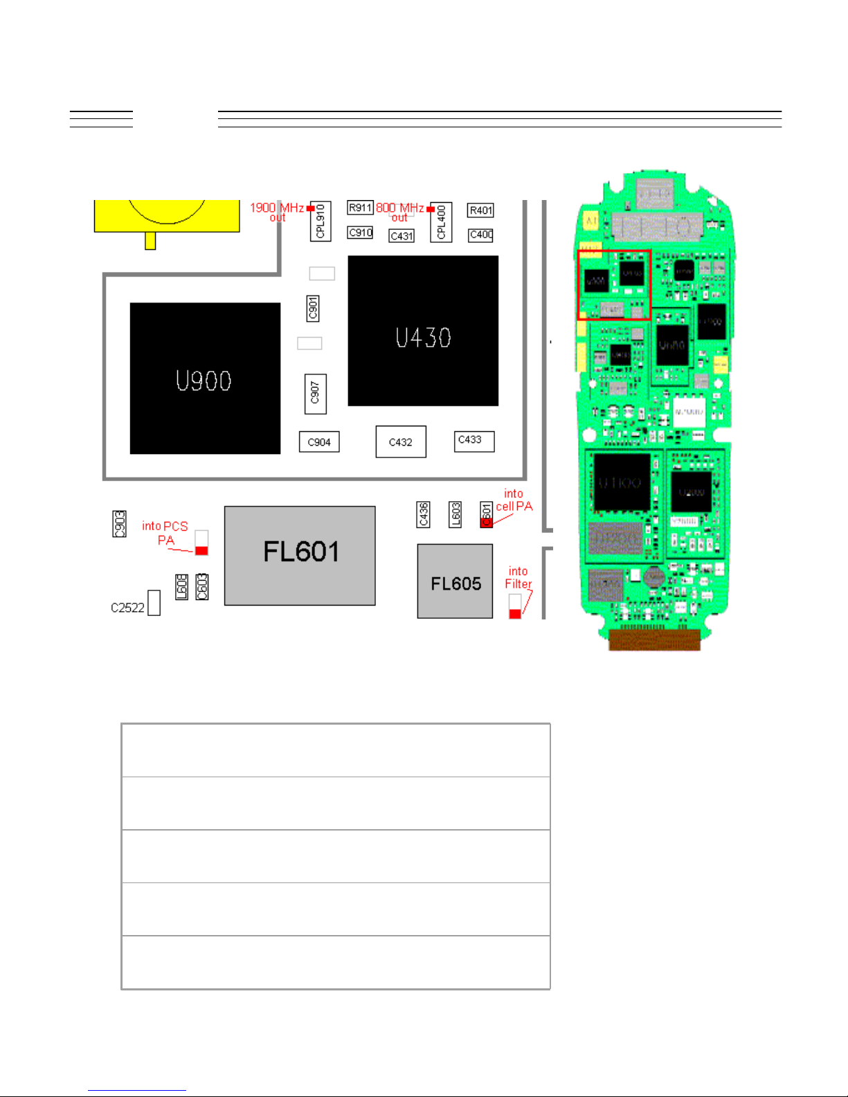
V.120c
Troubleshooting
C601
C638 (DNP)
CPL400 - 3
CPL910 - 3
L616 (DNP)
© 2001 Motorola, Inc. 24
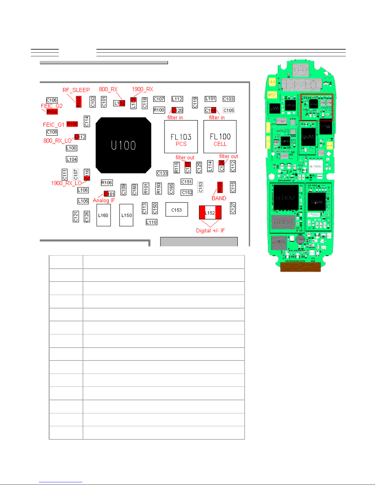
V.120c
Troubleshooting
C104 CELL LNA out to filter FL100
C116 1900_RX_LO to FEIC
C112
C120
C123
C124
C161
L102
L103
L152
R102
R104
R106
R108
© 2001 Motorola, Inc. 25
 Loading...