

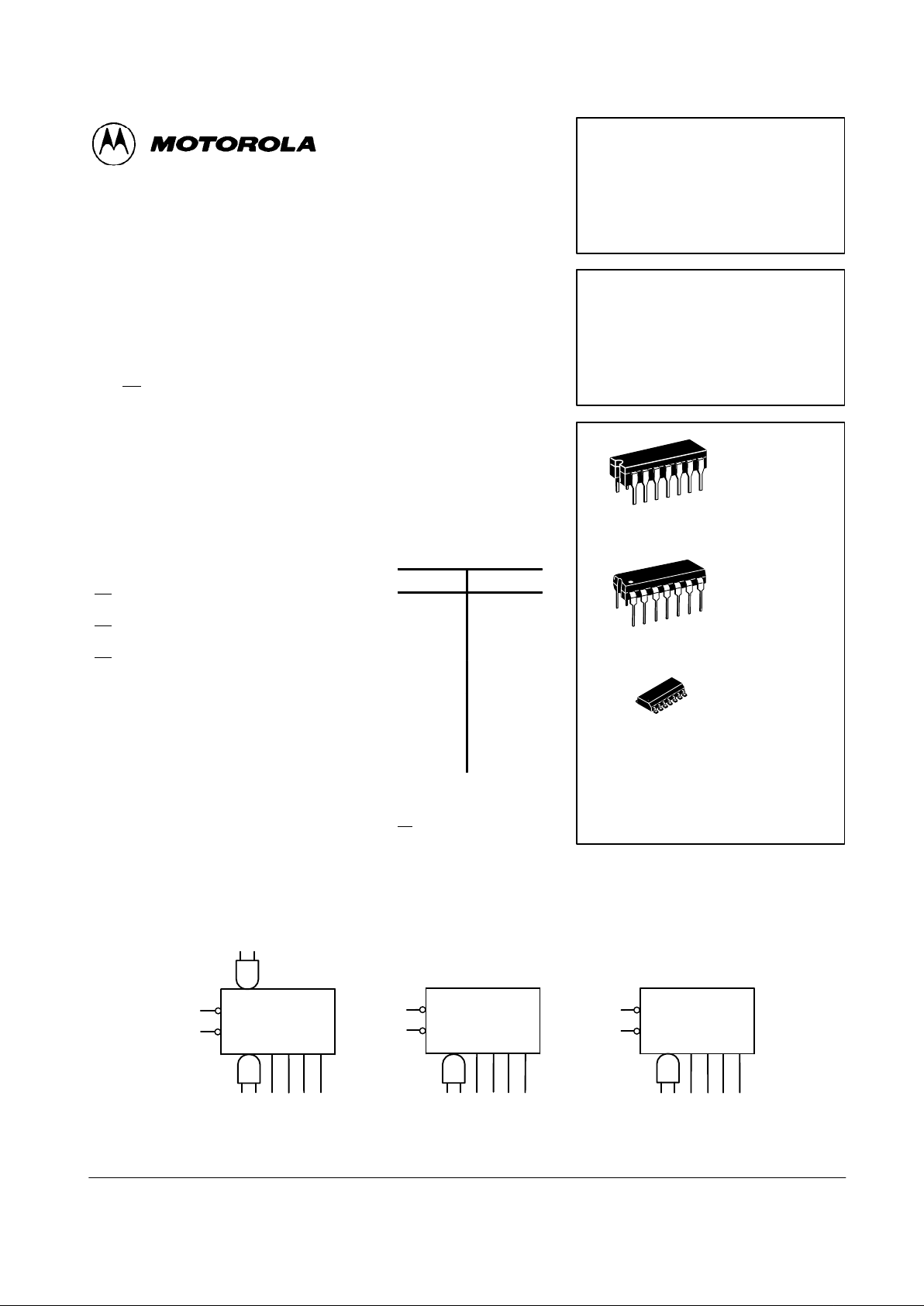
MOTOROLA SN74LS93DR2, SN74LS90DR2 Datasheet
5-1
FAST AND LS TTL DAT A
DECADE COUNTER;
DIVIDE-BY-TWELVE COUNTER;
4-BIT BINARY COUNTER
The SN54 /74LS90, SN54 /74LS92 and SN54 /74LS93 are high-speed
4-bit ripple type counters partitioned into two sections. Each counter has a divide-by-two section and either a divide-by-five (LS90), divide-by-six (LS92) or
divide-by-eight (LS93) section which are triggered by a HIGH-to-LOW transition on the clock inputs. Each section can be used separately or tied together
(Q to CP
) to form BCD, bi-quinary, modulo-12, or modulo-16 counters. All of
the counters have a 2-input gated Master Reset (Clear), and the LS90 also
has a 2-input gated Master Set (Preset 9).
• Low Power Consumption ...Typically 45 mW
• High Count Rates ...Typically 42 MHz
• Choice of Counting Modes . . . BCD, Bi-Quinary, Divide-by-Twelve,
Binary
• Input Clamp Diodes Limit High Speed Termination Effects
PIN NAMES LOADING (Note a)
HIGH
LOW
CP
0
Clock (Active LOW going edge) Input to
÷2 Section
0.5 U.L. 1.5 U.L.
CP
1
Clock (Active LOW going edge) Input to
÷5 Section (LS90), ÷6 Section (LS92)
0.5 U.L. 2.0 U.L.
CP
1
Clock (Active LOW going edge) Input to
÷8 Section (LS93)
0.5 U.L. 1.0 U.L.
MR1, MR2Master Reset (Clear) Inputs 0.5 U.L. 0.25 U.L.
MS1, MS2Master Set (Preset-9, LS90) Inputs 0.5 U.L. 0.25 U.L.
Q
0
Output from ÷2 Section (Notes b & c) 10 U.L. 5 (2.5) U.L.
Q1, Q2, Q3Outputs from ÷5 (LS90), ÷6 (LS92),
÷8 (LS93) Sections (Note b)
10 U.L. 5 (2.5) U.L.
NOTES:
a. 1 TTL Unit Load (U.L.) = 40 µA HIGH/1.6 mA LOW.
b. The Output LOW drive factor is 2.5 U.L. for Military, (54) and 5 U.L. for commercial (74)
b. T emperature Ranges.
c. The Q0 Outputs are guaranteed to drive the full fan-out plus the CP
1
input of the device.
d. T o insure proper operation the rise (tr) and fall time (tf) of the clock must be less than 100 ns.
SN54/74LS90
SN54/74LS92
SN54/74LS93
DECADE COUNTER;
DIVIDE-BY -TWELVE COUNTER;
4-BIT BINARY COUNTER
LOW POWER SCHOTTKY
J SUFFIX
CERAMIC
CASE 632-08
N SUFFIX
PLASTIC
CASE 646-06
14
1
14
1
ORDERING INFORMATION
SN54LSXXJ Ceramic
SN74LSXXN Plastic
SN74LSXXD SOIC
14
1
D SUFFIX
SOIC
CASE 751A-02
LOGIC SYMBOL
12
2
VCC = PIN 5
GND = PIN 10
NC = PINS 4, 13
VCC = PIN 5
GND = PIN 10
NC = PINS 2, 3, 4, 13
VCC = PIN 5
GND = PIN 10
NC = PIN 4, 6, 7, 13
LS90 LS92 LS93
67
12
14
1
12
23
MS
CP
0
CP
1
MR Q0Q1Q2Q
3
12 9 8 11 6 7
14
1
1
CP
0
CP
1
MR Q0Q1Q2Q
3
12 9 811
14
1
23
CP
0
CP
1
MR Q0Q1Q2Q
3
12 9 8 11
5-2
FAST AND LS TTL DATA
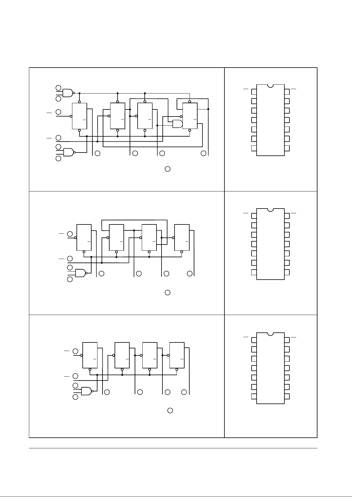
SN54/74LS90 • SN54/74LS92 • SN54/74LS93
LOGIC DIAGRAM
MS
1
MS
2
MR
1
MR
2
CP
0
CP
1
Q
0
Q
1
Q
2
Q
3
MR
1
CP
0
CP
1
Q
0
Q
1
Q
2
Q
3
MR
2
LS90
MR
1
CP
0
CP
1
Q
0
Q
1
Q
2
Q
3
MR
2
S
D
J
CP
KQQ
C
D
S
D
R
CP
SQQ
C
D
S
D
J
CP
KQQ
C
D
S
D
J
CP
KQQ
C
D
J
CP
KQQ
C
D
J
CP
KQQ
C
D
J
CP
KQQ
C
D
J
CP
KQQ
C
D
J
CP
KQQ
C
D
J
CP
KQQ
C
D
J
CP
KQQ
C
D
J
CP
KQQ
C
D
14
1112
1
2
6
7
9
3
8
14
13
12
11
10
9
1
2
3
4
5
6
87
CP
0
NC
Q
0
Q
3
GND
Q
1
Q
2
CP
1
MR
1
MR
2
NC
V
CC
MS
1
MS
2
CONNECTION DIAGRAM
DIP (TOP VIEW)
NC = NO INTERNAL CONNECTION
NOTE:
The Flatpak version has the same
pinouts (Connection Diagram) as
the Dual In-Line Package.
14
1
6
7
12 11 9 8
LOGIC DIAGRAM
LS92
14
13
12
11
10
9
1
2
3
4
5
6
87
CP
0
NC
Q
0
Q
1
GND
Q
2
Q
3
CP
1
NC
NC
NC
V
CC
MR
1
MR
2
CONNECTION DIAGRAM
DIP (TOP VIEW)
NC = NO INTERNAL CONNECTION
NOTE:
The Flatpak version has the same
pinouts (Connection Diagram) as
the Dual In-Line Package.
LOGIC DIAGRAM
LS93
VCC = PIN 5
GND = PIN 10
= PIN NUMBERS
VCC = PIN 5
GND = PIN 10
= PIN NUMBERS
VCC = PIN 5
GND = PIN 10
= PIN NUMBERS
14
1
2
3
12 9 8 11
14
13
12
11
10
9
1
2
3
4
5
6
87
CP
0
NC
Q
0
Q
3
GND
Q
1
Q
2
CP
1
MR
1
MR
2
NC
V
CC
NC
NC
CONNECTION DIAGRAM
DIP (TOP VIEW)
NC = NO INTERNAL CONNECTION
NOTE:
The Flatpak version has the same
pinouts (Connection Diagram) as
the Dual In-Line Package.
 Loading...