

5-84
FAST AND LS TTL DATA
4-BIT MAGNITUDE
COMPARATOR
The SN54/74LS85 is a 4-Bit Magnitude Camparator which compares two
4-bit words (A, B), each word having four Parallel Inputs (A0–A3, B0–B3); A3,
B3 being the most significant inputs. Operation is not restricted to binary
codes, the device will work with any monotonic code. Three Outputs are
provided: “A greater than B” (O
A>B
), “A less than B” (O
A<B
), “A equal to B”
(O
A=B
). Three Expander Inputs, I
A>B
, I
A<B
, I
A=B
, allow cascading without
external gates. For proper compare operation, the Expander Inputs to the
least significant position must be connected as follows: I
A<B
= I
A>B
= L, I
A=B
= H. For serial (ripple) expansion, the O
A>B
, O
A<B
and O
A=B
Outputs are
connected respectively to the I
A>B
, I
A<B
, and I
A=B
Inputs of the next most
significant comparator, as shown in Figure 1. Refer to Applications section of
data sheet for high speed method of comparing large words.
The Truth Table on the following page describes the operation of the
SN54/74LS85 under all possible logic conditions. The upper 11 lines describe
the normal operation under all conditions that will occur in a single device or
in a series expansion scheme. The lower five lines describe the operation
under abnormal conditions on the cascading inputs. These conditions occur
when the parallel expansion technique is used.
• Easily Expandable
• Binary or BCD Comparison
• O
A>B
, O
A<B
, and O
A=B
Outputs Available
CONNECTION DIAGRAM DIP (TOP VIEW)
NOTE:
The Flatpak version has the
same pinouts (Connection
Diagram) as the Dual In-Line
Package.
14 13 12 11 10 9
1 2 3 4 5 6
7
16 15
8
V
CC
B
3
A
3
B2A2A
1
A
0
B
1
B
0
I
A<BIA=BIA>BOA>BOA=B
O
A<B
GND
PIN NAMES LOADING (Note a)
HIGH
LOW
A0–A3, B0–B
3
I
A=B
I
A<B
, I
A>B
O
A>B
O
A<B
O
A=B
Parallel Inputs
A = B Expander Inputs
A < B, A > B, Expander Inputs
A Greater Than B Output (Note b)
B Greater Than A Output (Note b)
A Equal to B Output (Note b)
1.5 U.L.
1.5 U.L.
0.5 U.L.
10 U.L.
10 U.L.
10 U.L.
0.75 U.L.
0.75 U.L.
0.25 U.L.
5 (2.5) U.L.
5 (2.5) U.L.
5 (2.5) U.L.
NOTES:
a) 1 TTL Unit Load (U.L.) = 40 µA HIGH/1.6 mA LOW.
b) The Output LOW drive factor is 2.5 U.L. for Military (54) and 5 U.L. for Commercial (74)
Temperature Ranges.
SN54/74LS85
4-BIT MAGNITUDE
COMPARATOR
LOW POWER SCHOTTKY
J SUFFIX
CERAMIC
CASE 620-09
N SUFFIX
PLASTIC
CASE 648-08
16
1
16
1
ORDERING INFORMATION
SN54LSXXJ Ceramic
SN74LSXXN Plastic
SN74LSXXD SOIC
16
1
D SUFFIX
SOIC
CASE 751B-03
LOGIC SYMBOL
VCC = PIN 16
GND = PIN 8
10 12 1315 9 11 14 1
4
2
3
5
7
6
A0A1A2A3B0B1B2B
3
I
A>B
I
A<B
I
A=B
O
A>B
O
A<B
O
A=B
H = HIGH Level
L = LOW Level
X = IMMATERIAL
5-85
FAST AND LS TTL DATA
SN54/74LS85
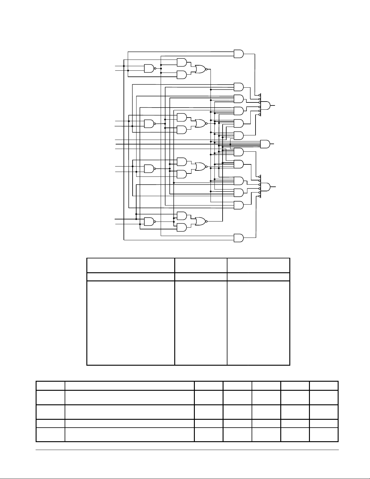
LOGIC DIAGRAM
O
A>B
O
A<B
O
A=B
(5)
(6)
(7)
A3
B3
A2
B2
A<B
A=B
A>B
A1
B1
A0
B0
(15)
(1)
(13)
(14)
(12)
(11)
(10)
(9)
(2)
(3)
(4)
TRUTH TABLE
COMPARING INPUTS
CASCADING
INPUTS
OUTPUTS
A3,B3A2,B2A1,B1A0,B0I
A>BIA<BIA=BOA>BOA<BOA=B
A3>B
3
X X X X X X H L L
A3<B
3
X X X X X X L H L
A3=B3A2>B
2
X X X X X H L L
A3=B3A2<B
2
X X X X X L H L
A3=B3A2=B2A1>B
1
X X X X H L L
A3=B3A2=B2A1<B
1
X X X X L H L
A3=B3A2=B2A1=B1 A0>B
0
X X X H L L
A3=B3A2=B2A1=B1A0<B
0
X X X L H L
A3=B3A2=B2A1=B1A0=B
0
H L L H L L
A3=B3A2=B2A1=B1A0=B
0
L H L L H L
A3=B3A2=B2A1=B1A0=B
0
X X H L L H
A3=B3A2=B2A1=B1A0=B
0
H H L L L L
A3=B3A2=B2A1=B1A0=B
0
L L L H H L
GUARANTEED OPERATING RANGES
Symbol Parameter Min Typ Max Unit
V
CC
Supply Voltage 54
74
4.5
4.75
5.0
5.0
5.5
5.25
V
T
A
Operating Ambient Temperature Range 54
74
–55
0
25
25
125
70
°C
I
OH
Output Current — High 54, 74 –0.4 mA
I
OL
Output Current — Low 54
74
4.0
8.0
mA
NOTE:
The SN54/74LS85 can be used as a 5-bit comparator
only when the outputs are used to drive the A0–A3 and
B0–B3 inputs of another SN54/74LS85 as shown in
Figure 2 in positions #1, 2, 3, and 4.
5-86
FAST AND LS TTL DATA
SN54/74LS85
Figure 1. Comparing Two n-Bit Words
L = LOW LEVEL
H = HIGH LEVEL
A0A1A2A3B0B1B2B
3
A0A1A2A3B0B1B2B
3
A0A1A2A3B0B1B2B
3
L
L
H
IA >
B
IA <
B
IA =
B
OA >
B
OA <
B
OA =
B
IA >
B
IA <
B
IA =
B
OA >
B
OA <
B
OA =
B
A > B
A < B
A = B
SN54/74LS85 SN54/74LS85
An3An2An1AnBn3Bn2Bn1B
n
APPLICATIONS
Figure 2 shows a high speed method of comparing two 24-bit words with only two levels of device delay. With the technique
shown in Figure 1, six levels of device delay result when comparing two 24-bit words. The parallel technique can be expanded
to any number of bits, see Table 1.
Table 1
WORD LENGTH NUMBER OF PKGS.
1–4 Bits 1
5–24 Bits 2–6
25–120 Bits 8–31
MSB = MOST SIGNIFICANT BIT
LSB = LEAST SIGNIFICANT BIT
L = LOW LEVEL
H = HIGH LEVEL
NC = NO CONNECTION
A0A1A2A3B0B1B2B
3
A0A1A2A3B0B1B2B
3
L
L
H
IA >
B
IA <
B
IA =
B
OA >
B
OA <
B
OA =
B
#5
(LSB)
INPUTS
A0A1A2A3B0B1B2B
3
IA >
B
IA <
B
IA =
B
OA >
B
OA <
B
OA =
B
#1
L
NC
A20A
21
B23B22B21B20A23A
22
A
19
B
19
(MSB)
A5A6A7A8B5B6B7B
8
A0A1A2A3B0B1B2B
3
IA >
B
IA <
B
IA =
B
OA >
B
OA <
B
OA =
B
#4
NC
L
A
4
B
4
A0A1A2A3B0B1B2B
3
IA >
B
IA <
B
IA =
B
OA >
B
OA <
B
OA =
B
#3
NC
L
A
9
B
9
A10A
11
B13B12B11B10A13A
12
A0A1A2A3B0B1B
2
B
3
IA >
B
IA <
B
IA =
B
OA >
B
OA <
B
OA =
B
#2
NC
L
A
14
B
14
A15A
16
B18B17B16B15A18A
17
OUTPUTS
A0A1A2A3B0B1B2B
3
IA >
B
IA <
B
IA =
B
OA >
B
OA <
B
OA =
B
#6
INPUTS
Figure 2. Comparison of Two 24-Bit Words

5-87
FAST AND LS TTL DATA
SN54/74LS85
DC CHARACTERISTICS OVER OPERATING TEMPERATURE RANGE (unless otherwise specified)
Limits
Symbol
Parameter
Min Typ Max
Unit
Test Conditions
V
IH
Input HIGH Voltage 2.0 V
Guaranteed Input HIGH Voltage for
All Inputs
54 0.7
VILInput LOW Voltage
74 0.8
V
Guaranteed Input LOW Voltage for
All Inputs
V
IK
Input Clamp Diode Voltage –0.65 –1.5 V VCC = MIN, IIN = –18 mA
54
2.5
3.5
V
VCC = MIN, IOH = MAX, VIN = V
IH
VOHOutput HIGH Voltage
74 2.7 3.5 V
VCC = MIN, IOH = MAX, VIN = V
IH
or VIL per Truth Table
54, 74 0.25
0.4
V IOL = 4.0 mA
VOLOutput LOW Voltage
74 0.35 0.5 V
IOL = 8.0 mA
VIN = VIL or V
IH
per Truth Table
Input HIGH Current
A < B, A > B
Other Inputs
20
60
µA VCC = MAX, VIN = 2.7 V
I
IH
A < B, A > B
Other Inputs
0.1
0.3
mA VCC = MAX, VIN = 7.0 V
I
IL
Input LOW Current
A < B, A > B
Other Inputs
–0.4
–1.2
mA VCC = MAX, VIN = 0.4 V
I
OS
Output Short Circuit Current (Note 1) –20 –100 mA VCC = MAX
I
CC
Power Supply Current 20 mA VCC = MAX
Note 1: Not more than one output should be shorted at a time, nor for more than 1 second.
AC CHARACTERISTICS (T
A
= 25°C, VCC = 5.0 V)
Limits
Symbol
Parameter
Min Typ Max
Unit
Test Conditions
t
PLH
t
PHL
Any A or B to A < B, A > B 24
20
36
30
ns
t
PLH
t
PHL
Any A or B to A = B 27
23
45
45
ns
t
PLH
t
PHL
A < B or A = B to A > B 14
11
22
17
ns
t
PLH
t
PHL
A = B to A = B 13
13
20
26
ns
t
PLH
t
PHL
A > B or A = B to A < B 14
11
22
17
ns
Figure 3
Figure 4
AC WAVEFORMS
V
IN
V
OUT
1.3 V
t
PHL
1.3 V
1.3 V
1.3 V
t
PLH
V
IN
V
OUT
1.3 V
t
PHL
1.3 V
1.3 V 1.3 V
t
PLH
I
Guaranteed Input LOW Voltage for
VCC = VCC MIN,
VCC = 5.0 V
CL = 15 pF
 Loading...