

MOTOROLA SN74LS74AM, SN74LS74AMEL, SN74LS74AML1, SN74LS74AML2, SN74LS74AMR1 Datasheet
...
Semiconductor Components Industries, LLC, 1999
December, 1999 – Rev. 6
1 Publication Order Number:
SN74LS74A/D
SN74LS74A
Dual D-Type Positive
Edge-Trigger ed Flip-Flop
The SN74LS74A dual edge-triggered flip-flop utilizes Schottky
TTL circuitry to produce high speed D-type flip-flops. Each flip-flop
has individual clear and set inputs, and also complementary Q and Q
outputs.
Information at input D is transferred to the Q output on the
positive-going edge of the clock pulse. Clock triggering occurs at a
voltage level of the clock pulse and is not directly related to the
transition time of the positive-going pulse. When the clock input is at
either the HIGH or the LOW level, the D input signal has no effect.
MODE SELECT – TRUTH TABLE
INPUTS OUTPUTS
OPERATING MODE
S
D
S
D
D Q Q
Set
Reset (Clear)
*Undetermined
Load “1” (Set)
Load “0” (Reset)
L
H
L
H
H
H
L
L
H
H
X
X
X
h
l
H
L
H
H
L
L
H
H
L
H
* Both outputs will be HIGH while both SD and CD are LOW, but the output
states are unpredictable if S
D
and CD go HIGH simultaneously. If the levels
at the set and clear are near V
IL
maximum then we cannot guarantee to meet
the minimum level for V
OH
.
H, h = HIGH Voltage Level
L, I = LOW Voltage Level
X = Don’t Care
l, h (q) = Lower case letters indicate the state of the referenced input
i, h (q) = (or output) one set-up time prior to the HIGH to LOW clock transition.
GUARANTEED OPERATING RANGES
Symbol Parameter Min Typ Max Unit
V
CC
Supply Voltage 4.75 5.0 5.25 V
T
A
Operating Ambient
T emperature Range
0 25 70 °C
I
OH
Output Current – High –0.4 mA
I
OL
Output Current – Low 8.0 mA
LOW
POWER
SCHOTTKY
Device Package Shipping
ORDERING INFORMATION
SN74LS74AN 14 Pin DIP 2000 Units/Box
SN74LS74AD 14 Pin
SOIC
D SUFFIX
CASE 751A
http://onsemi.com
2500/Tape & Reel
PLASTIC
N SUFFIX
CASE 646
14
1
14
1
SN74LS74A
http://onsemi.com
2
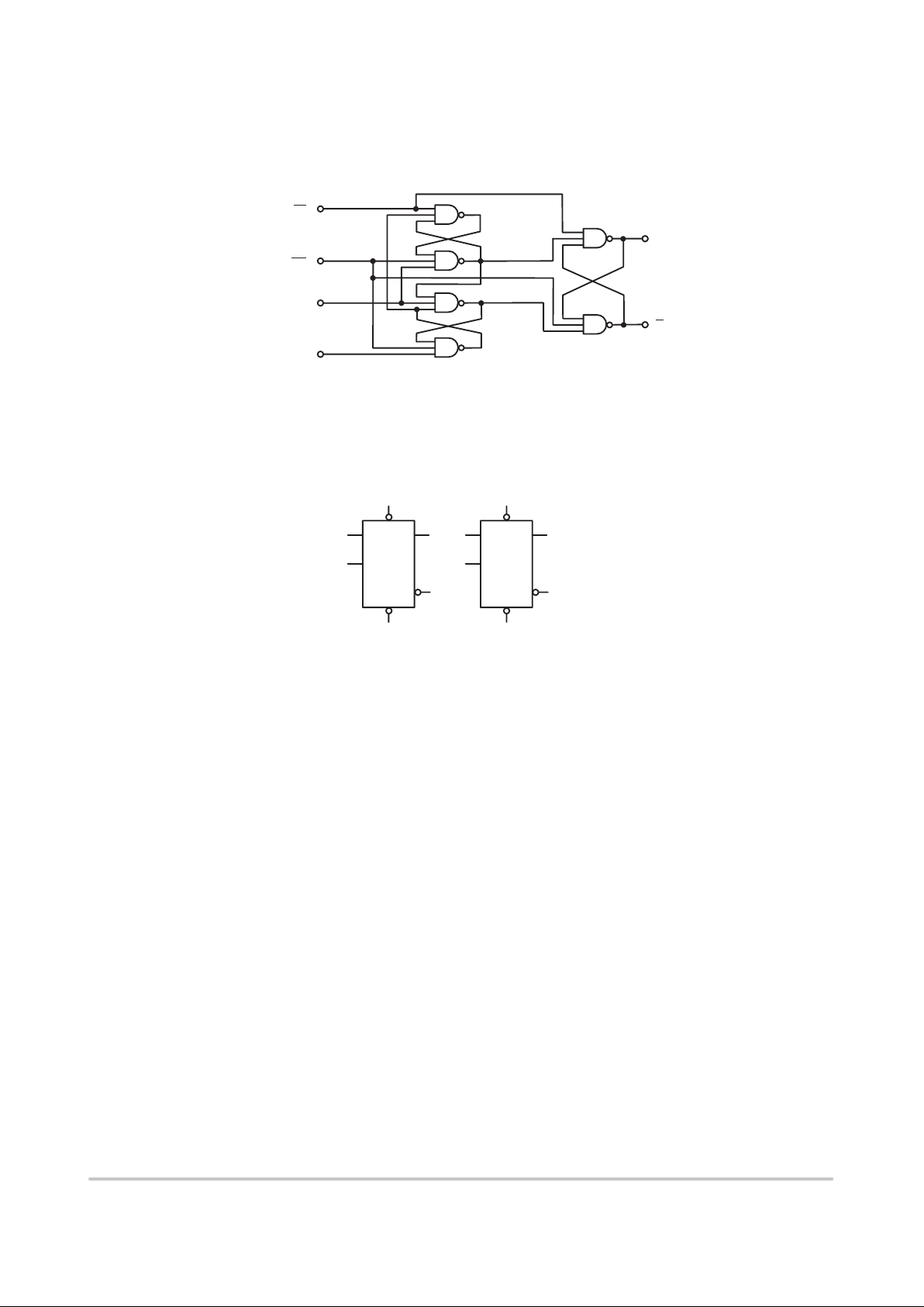
LOGIC DIAGRAM (Each Flip-Flop)
LOGIC SYMBOL
SET (SD)
4 (10)
CLEAR (CD
)
1 (13)
CLOCK
3 (11)
D
2 (12)
Q
5 (9)
Q
6 (8)
VCC = PIN 14
GND = PIN 7
2
3
5
DQ
CP
Q
C
D
1
4
6
12
11
9
DQ
CP
Q
C
D
13
10
8
S
D
S
D
SN74LS74A
http://onsemi.com
3
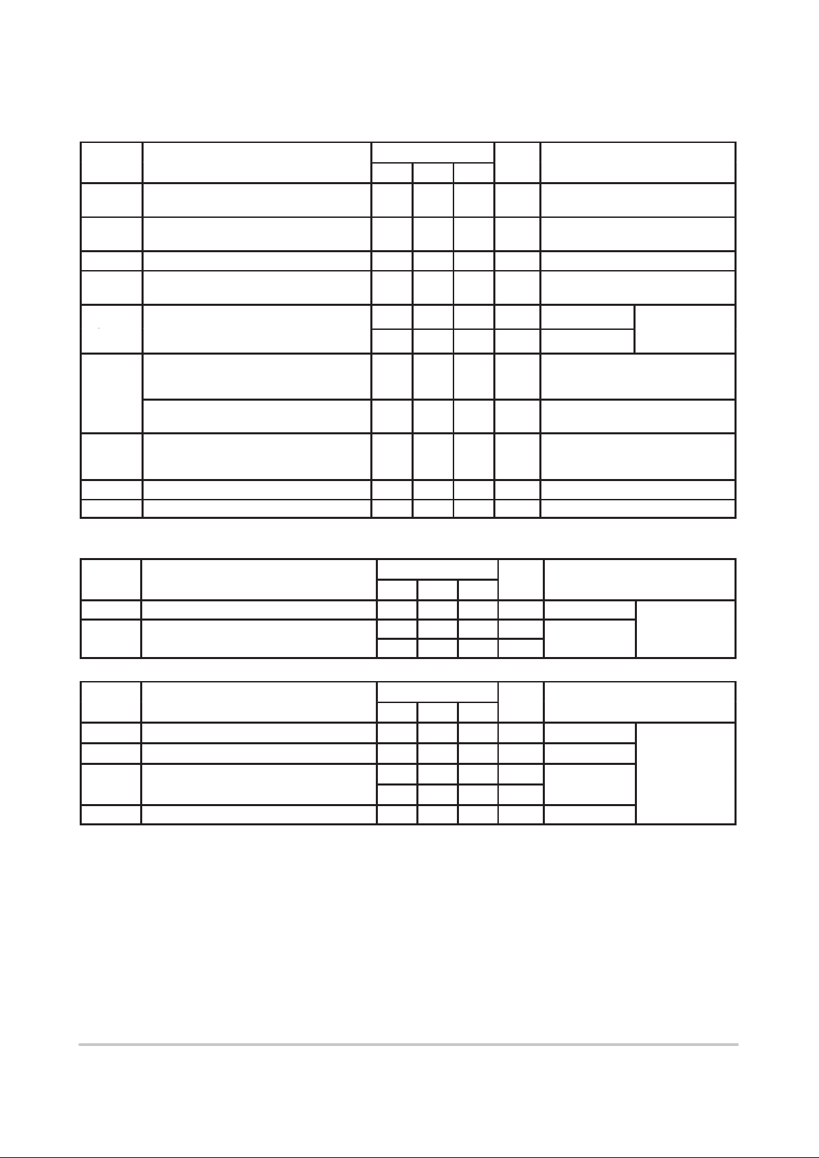
DC CHARACTERISTICS OVER OPERATING TEMPERATURE RANGE (unless otherwise specified)
Limits
Symbol Parameter
Min Typ Max
Unit Test Conditions
V
IH
Input HIGH Voltage 2.0 V
Guaranteed Input HIGH Voltage for
All Inputs
V
IL
Input LOW Voltage
0.8
V
Guaranteed Input LOW Voltage for
All Inputs
V
IK
Input Clamp Diode Voltage –0.65 –1.5 V VCC = MIN, IIN = –18 mA
V
OH
Output HIGH Voltage
2.7 3.5 V VCC = MIN, IOH = MAX, VIN = V
IH
or VIL per Truth Table
p
0.25 0.4 V IOL = 4.0 mA
VCC = VCC MIN,
VOLOutput LOW Voltage
0.35 0.5 V IOL = 8.0 mA
V
IN
=
V
IL
or
V
IH
per Truth Table
I
IH
Input High Current
Data, Clock
Set, Clear
20
40
µA VCC = MAX, VIN = 2.7 V
IH
Data, Clock
Set, Clear
0.1
0.2
mA VCC = MAX, VIN = 7.0 V
I
IL
Input LOW Current
Data, Clock
Set, Clear
–0.4
–0.8
mA VCC = MAX, VIN = 0.4 V
I
OS
Output Short Circuit Current (Note 1) –20 –100 mA VCC = MAX
I
CC
Power Supply Current 8.0 mA VCC = MAX
Note 1: Not more than one output should be shorted at a time, nor for more than 1 second.
AC CHARACTERISTICS (T
A
= 25°C, VCC = 5.0 V)
Limits
Symbol Parameter
Min Typ Max
Unit Test Conditions
f
MAX
Maximum Clock Frequency 25 33 MHz Figure 1
t
PLH
p
13 25 ns
VCC = 5.0 V
=
p
PLH
t
PHL
Clock, Clear, Set to Output
25 40 ns
Figure 1
C
L
= 15
F
AC SETUP REQUIREMENTS (T
A
= 25°C)
Limits
Symbol Parameter
Min Typ Max
Unit Test Conditions
t
W(H)
Clock 25 ns Figure 1
t
W(L)
Clear, Set 25 ns Figure 2
Data Setup Time — HIGH
20 ns
VCC = 5.0 V
t
s
Data Setup Time — LOW
20 ns
Figure 1
t
h
Hold Time 5.0 ns Figure 1
 Loading...