

Motorola SN54LS73AJ, SN74LS73AD, SN74LS73AN Datasheet
5-68
FAST AND LS TTL DATA
DUAL JK NEGATIVE
EDGE-TRIGGERED FLIP-FLOP
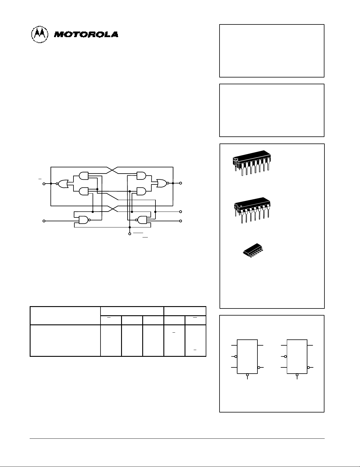
The SN54LS/74LS73A offers individual J, K, clear, and clock inputs. These
dual flip-flops are designed so that when the clock goes HIGH, the inputs are
enabled and data will be accepted. The logic level of the J and K inputs may
be allowed to change when the clock pulse is HIGH and the bistable will perform according to the truth table as long as minimum set-up times are observed. Input data is transferred to the outputs on the negative-going edge of
the clock pulse.
LOGIC DIAGRAM (Each Flip-Flop)
Q
K
13 (8)
3 (10)
Q
12 (9)
CLEAR
2 (6)
J
14 (7)
1 (15)
CLOCK (CP)
MODE SELECT — TRUTH TABLE
INPUTS OUTPUTS
OPERATING MODE
C
D
J K Q Q
Reset (Clear)
Toggle
Load “0” (Reset)
Load “1” (Set)
Hold
L
H
H
H
H
X
h
l
h
l
X
h
h
l
l
L
q
L
H
q
H
q
H
L
q
H, h = HIGH Voltage Level
L, I = LOW Voltage Level
X = Don’t Care
l, h (q) = Lower case letters indicate the state of the referenced input (or output) one set-up time
l, h (q) = prior to the HIGH to LOW clock transition.
SN54/74LS73A
DUAL JK NEGATIVE
EDGE-TRIGGERED FLIP-FLOP
LOW POWER SCHOTTKY
J SUFFIX
CERAMIC
CASE 632-08
N SUFFIX
PLASTIC
CASE 646-06
14
1
14
1
ORDERING INFORMATION
SN54LSXXJ Ceramic
SN74LSXXN Plastic
SN74LSXXD SOIC
14
1
D SUFFIX
SOIC
CASE 751A-02
LOGIC SYMBOL
14
1
3
12
13
J Q
CP
K Q
C
D
2
VCC = PIN 4
GND = PIN 11
7
5
10
9
8
J Q
CP
K Q
C
D
6
5-69
FAST AND LS TTL DATA
SN54/74LS73A
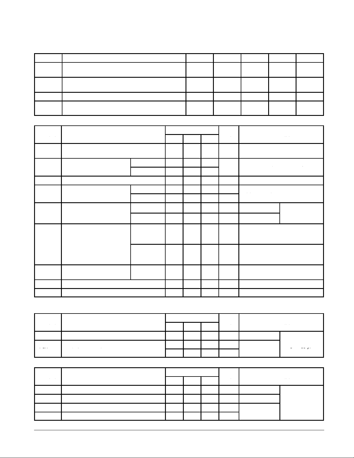
GUARANTEED OPERATING RANGES
Symbol Parameter Min Typ Max Unit
V
CC
Supply Voltage 54
74
4.5
4.75
5.0
5.0
5.5
5.25
V
T
A
Operating Ambient Temperature Range 54
74
–55
0
25
25
125
70
°C
I
OH
Output Current — High 54, 74 –0.4 mA
I
OL
Output Current — Low 54
74
4.0
8.0
mA
DC CHARACTERISTICS OVER OPERATING TEMPERATURE RANGE (unless otherwise specified)
Limits
Symbol
Parameter
Min Typ Max
Unit
Test Conditions
V
IH
Input HIGH Voltage 2.0 V
Guaranteed Input HIGH Voltage for
All Inputs
54 0.7
VILInput LOW Voltage
74 0.8
V
Guaranteed Input LOW Voltage for
All Inputs
V
IK
Input Clamp Diode Voltage –0.65 –1.5 V VCC = MIN, IIN = –18 mA
54 2.5 3.5 V
CC
= MIN, IOH = MAX, VIN = V
IH
VOHOutput HIGH Voltage
74 2.7 3.5 V
VCC = MIN, IOH = MAX, VIN = V
IH
or VIL per Truth Table
54, 74 0.25 0.4 V IOL = 4.0 mA
VOLOutput LOW Voltage
74 0.35 0.5 V IOL = 8.0 mA
VIN = VIL or V
IH
per Truth Table
J, K
Clear
Clock
20
60
80
µA VCC = MAX, VIN = 2.7 V
IIHInput HIGH Current
J, K
Clear
Clock
0.1
0.3
0.4
mA VCC = MAX, VIN = 7.0 V
I
IL
Input LOW Current
J, K
Clear, Clock
–0.4
–0.8
mA VCC = MAX, VIN = 0.4 V
I
OS
Short Circuit Current (Note 1) –20 –100 mA VCC = MAX
I
CC
Power Supply Current 6.0 mA VCC = MAX
Note 1: Not more than one output should be shorted at a time, nor for more than 1 second.
AC CHARACTERISTICS (T
A
= 25°C, VCC = 5.0 V)
Limits
Symbol
Parameter
Min Typ Max
Unit
Test Conditions
f
MAX
Maximum Clock Frequency 30 45 MHz Figure 1
PLH
15 20 ns
VCC = 5.0 V
C
= 15 pF
t
PLH
t
PHL
Propagation Delay,
Clock to Output
15 20 ns
Figure 1
CL = 15 pF
AC SETUP REQUIREMENTS (T
A
= 25°C)
Limits
Symbol
Parameter
Min Typ Max
Unit
Test Conditions
t
W
Clock Pulse Width High 20 ns Figure 1
t
W
Clear Pulse Width 25 ns Figure 2
t
s
Setup Time 20 ns
VCC = 5.0 V
t
h
Hold Time 0 ns
Figure 1
Guaranteed Input LOW Voltage for
V
VCC = VCC MIN,
t
Propagation Delay,
 Loading...