

MOTOROLA SN74LS688DW, SN74LS688DWR2, SN74LS684DWR2, SN74LS684H, SN74LS684MEL Datasheet
...
Semiconductor Components Industries, LLC, 1999
December, 1999 – Rev. 6
1 Publication Order Number:
SN74LS682/D
SN74LS682 SN74LS684
SN74LS688
8-Bit Magnitude
Comparators
The SN74LS682, 684, 688 are 8-bit magnitude comparators. These
device types are designed to perform comparisons between two
eight-bit binary or BCD words. All device types provide P = Q
outputs
and the LS682 and LS684 have P>Q outputs also.
The LS682, LS684 and LS688 are totem pole devices. The LS682
has a 20 kΩ pullup resistor on the Q inputs for analog or switch data.
OUTPUT OUTPUT
TYPE P = Q P > Q
ENABLE CONFIGURATION
PULLUP
LS682 yes yes no totem-pole yes
LS684 yes yes no totem-pole no
LS688 yes no yes totem-pole no
GUARANTEED OPERATING RANGES
Symbol Parameter Min Typ Max Unit
V
CC
Supply Voltage 4.75 5.0 5.25 V
T
A
Operating Ambient
T emperature Range
0 25 70 °C
I
OH
Output Current – High – 0.4 mA
I
OL
Output Current – Low 24 mA
LOW
POWER
SCHOTTKY
Device Package Shipping
ORDERING INFORMATION
SN74LS682N 16 Pin DIP 1440 Units/Box
SN74LS682DW 16 Pin
SOIC
DW SUFFIX
CASE 751D
http://onsemi.com
2500/Tape & Reel
PLASTIC
N SUFFIX
CASE 738
20
1
20
1
SN74LS684N 16 Pin DIP 1440 Units/Box
SN74LS684DW 16 Pin
2500/Tape & Reel
SN74LS688N 16 Pin DIP 1440 Units/Box
SN74LS688DW 16 Pin
2500/Tape & Reel
SN74LS682 SN74LS684 SN74LS688
http://onsemi.com
2
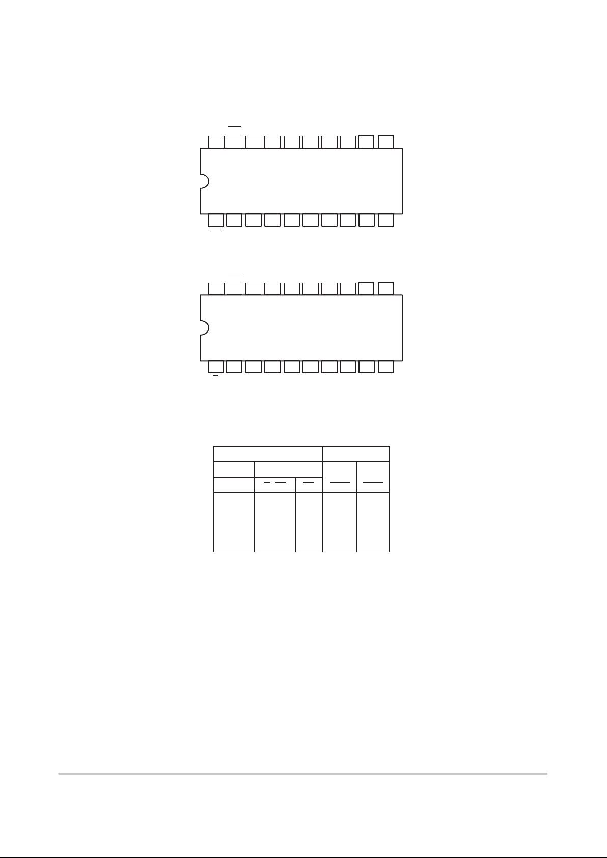
CONNECTION DIAGRAMS (TOP VIEW)
SN74LS682/684
18 17 16 15 14 13
123456
7
20 19
8
V
CC
P>Q
P=Q Q7 P7 Q6 Q5P6 P5
P0 Q0 P1 Q1 P2 Q2 P3
910
Q3 GND
12 11
Q4 P4
SN74LS688
18 17 16 15 14 13
123456
7
20 19
8
V
CC
G
P=Q Q7 P7 Q6 Q5P6 P5
P0 Q0 P1 Q1 P2 Q2 P3
910
Q3 GND
12 11
Q4 P4
FUNCTION TABLE
INPUTS OUTPUTS
DATA ENABLES
P, Q G
, GT G2 P = Q P > Q
P = Q
P > Q
P < Q
X
L
L
L
H
L
L
L
H
L
H
H
H
H
L
H
H
H = HIGH Level, L = LOW Level, X = Irrelevant
SN74LS682 SN74LS684 SN74LS688
http://onsemi.com
3
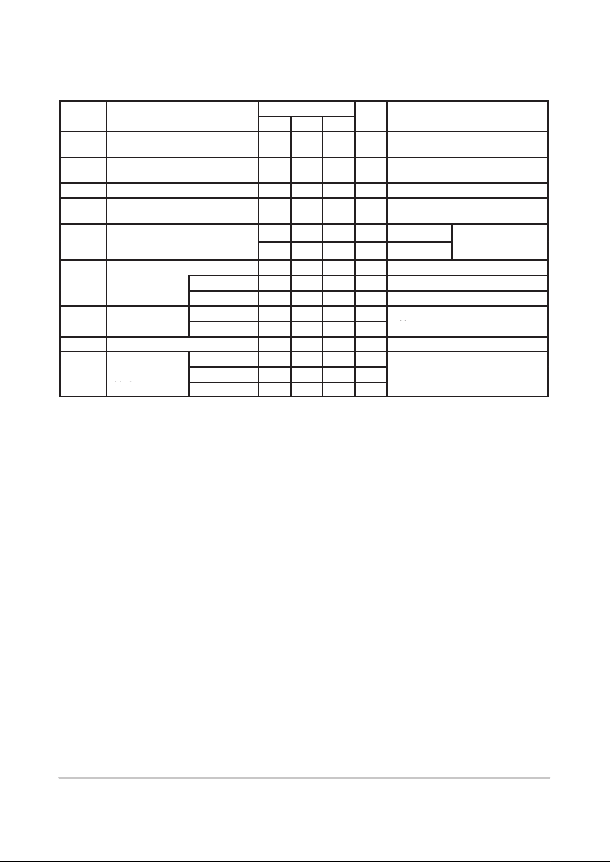
DC CHARACTERISTICS OVER OPERATING TEMPERATURE RANGE (unless otherwise specified)
Limits
Symbol Parameter
Min Typ Max
Unit Test Conditions
V
IH
Input HIGH Voltage 2.0 V
Guaranteed Input HIGH Voltage for
All Inputs
V
IL
Input LOW Voltage
0.8
V
Guaranteed Input LOW Voltage for
All Inputs
V
IK
Input Clamp Diode Voltage –0.65 –1.5 V VCC = MIN, IIN = –18 mA
V
OH
Output HIGH Voltage 2.7 3.5 V VCC = MIN, IOH = MAX, VIN = V
IH
or VIL per Truth Table
p
0.25 0.4 V IOL = 12 mA
VCC = VCC MIN,
VOLOutput LOW Voltage
0.35 0.5 V IOL = 24 mA
V
IN
=
V
IL
or
V
IH
per Truth Table
20 µA VCC = MAX, VIN = 2.7 V
I
IH
Input HIGH Current
LS682-Q Inputs 0.1 mA VCC = MAX, VIN = 5.5 V
Others 0.1 mA VCC = MAX, VIN = 7.0 V
p
LS682-Q Inputs –0.4 mA
IILInput LOW Current
Others –0.2 mA
V
CC
=
MAX, V
IN
= 0.4
V
I
OS
Short Circuit Current (Note 1) –30 –130 mA VCC = MAX
LS682 70 mA
I
CC
Power Supply
Current
LS684 65 mA
VCC = MAX
Current
LS688 65 mA
Note 1: Not more than one output should be shorted at a time, nor for more than 1 second.
 Loading...