

MOTOROLA SN74LS670N, SN74LS670D Datasheet
SN74LS670
4 x 4 Register File
with 3-State Outputs
The TTL/MSI SN74LS670 is a high-speed, low-power 4 x 4
Register File organized as four words by four bits. Separate read and
write inputs, both address and enable, allow simultaneous read and
write operation.
The 3-state outputs make it possible to connect up to 128 outputs to
increase the word capacity up to 512 words. Any number of these
devices can be operated in parallel to generate an n-bit length.
• Simultaneous Read/Write Operation
• Expandable to 512 Words by n-Bits
• T ypical Access Time to 20 ns
• 3-State Outputs for Expansion
• T ypical Power Dissipation of 125 mW
http://onsemi.com
LOW
POWER
SCHOTTKY
GUARANTEED OPERATING RANGES
Symbol Parameter Min Typ Max Unit
V
CC
T
I
OH
I
OL
Supply Voltage 4.75 5.0 5.25 V
Operating Ambient
A
T emperature Range
Output Current – High –2.6 mA
Output Current – Low 24 mA
0 25 70 °C
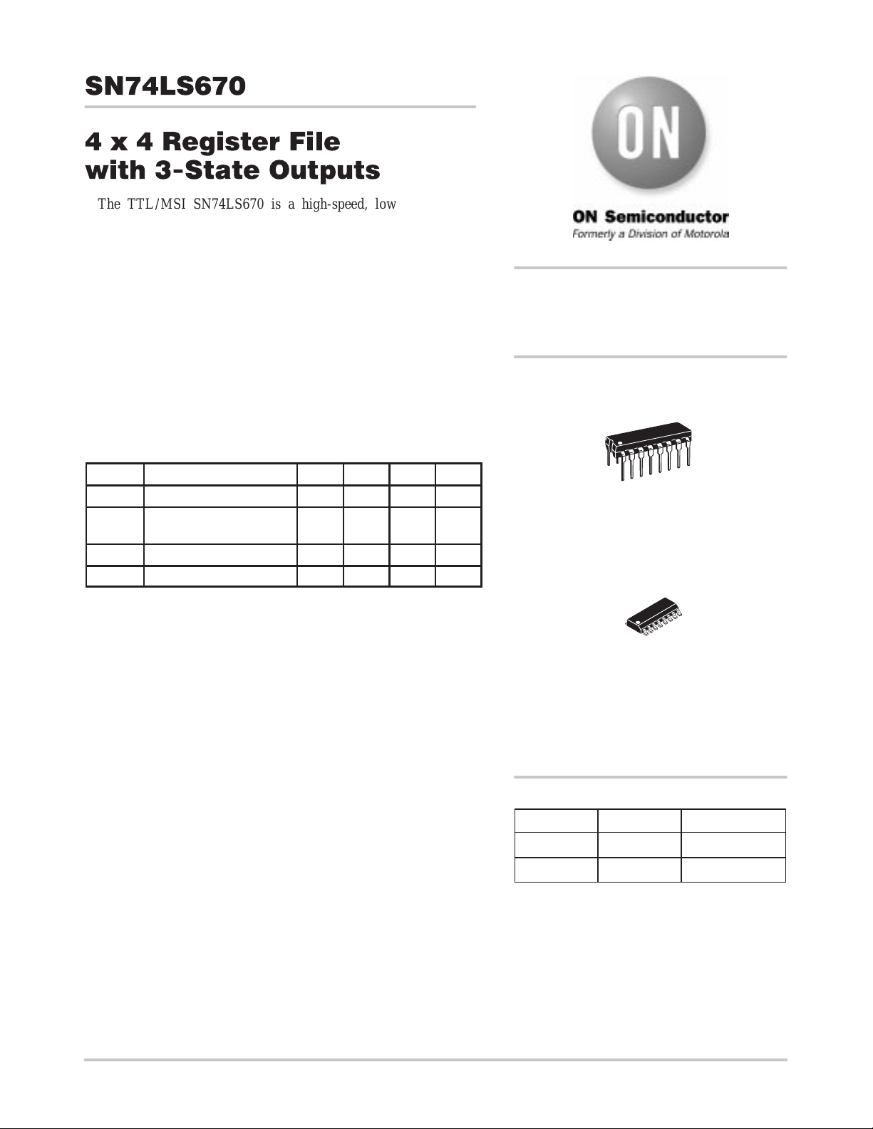
16
1
PLASTIC
N SUFFIX
CASE 648
16
1
SOIC
D SUFFIX
CASE 751B
ORDERING INFORMATION
Device Package Shipping
SN74LS670N 16 Pin DIP 2000 Units/Box
Semiconductor Components Industries, LLC, 1999
December, 1999 – Rev. 6
SN74LS670D 16 Pin
1 Publication Order Number:
2500/Tape & Reel
SN74LS670/D
SN74LS670
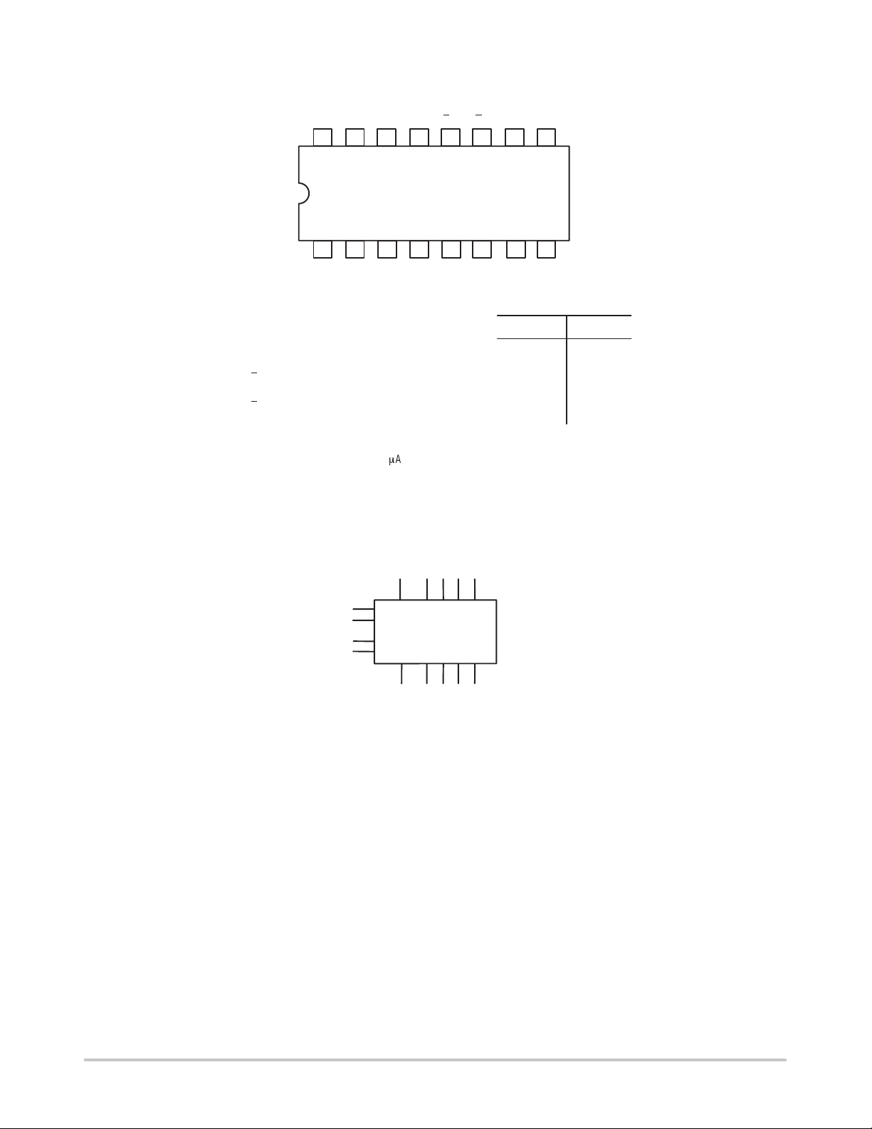
CONNECTION DIAGRAM DIP (TOP VIEW)
D1WAWBE
V
CC
16 15
W
14 13 12 11 10 9
Q
E
R
Q
1
2
NOTE:
The Flatpak version has the same
pinouts (Connection Diagram) as
the Dual In-Line Package.
123456
D
D3D4RBRAQ4Q3GND
2
PIN NAMES
D
– D
1
WA, W
E
W
RA, R
E
R
Q1 – Q
4
B
B
4
Data Inputs
Write Address Inputs
Write Enable (Active LOW) Input
Read Address Inputs
Read Enable (Active LOW) Input
Outputs
NOTES:
a) 1 TTL Unit Load (U.L.) = 40 mA HIGH/1.6 mA LOW.
LOGIC SYMBOL
12 15 1 2 3
D
W
1
Q1Q2Q3Q
R
D
2
14
13
5
4
E
W
A
W
B
R
A
R
B
E
D3D
7
HIGH LOW
0.5 U.L.
0.5 U.L.
1.0 U.L.
0.5 U.L.
1.5 U.L.
65 U.L.
4
4
8
(Note a)LOADING
0.25 U.L.
0.25 U.L.
0.5 U.L.
0.25 U.L.
0.75 U.L.
15 U.L.
11 10 9 7 6
= PIN 16
V
CC
GND = PIN 8
http://onsemi.com
2
SN74LS670
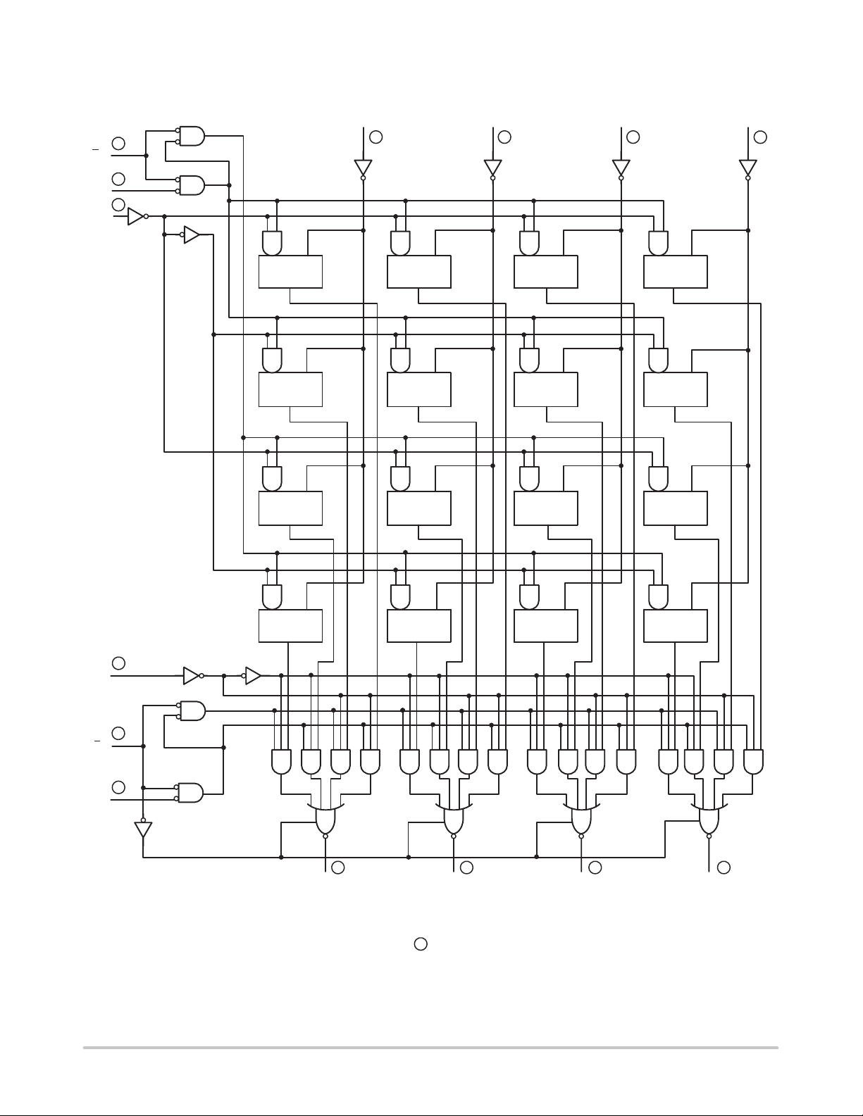
LOGIC DIAGRAM
D
4
12
E
W
13
W
B
14
W
A
3
D
3
D
2
12
D
1
15
WORD
0
GD
Q
GD
Q
GD
Q
GD
Q
WORD
GD
Q
GD
Q
GD
Q
GD
1
Q
WORD
2
GD
Q
GD
Q
GD
Q
GD
Q
WORD
3
GD
Q
4
R
B
11
E
R
5
R
A
67
Q
4
GD
Q
Q
3
GD
Q
Q
2
9
GD
Q
Q
10
1
VCC = PIN 16
GND = PIN 8
= PIN NUMBERS
http://onsemi.com
3
 Loading...