

Semiconductor Components Industries, LLC, 1999
December, 1999 – Rev. 6
1 Publication Order Number:
SN74LS221/D
SN74LS221
Dual Monostable
Multivibrators with
Schmitt-Trigger Inputs
Each multivibrator of the LS221 features a negative-transitiontriggered input and a positive-transition-triggered input either of
which can be used as an inhibit input.
Pulse triggering occurs at a voltage level and is not related to the
transition time of the input pulse. Schmitt-trigger input circuitry for B
input allows jitter-free triggering for inputs as slow as 1 volt /second,
providing the circuit with excellent noise immunity. A high immunity
to V
CC
noise is also provided by internal latching circuitry.
Once triggered, the outputs are independent of further transitions of
the inputs and are a function of the timing components. The output
pulses can be terminated by the overriding clear. Input pulse width
may be of any duration relative to the output pulse width. Output pulse
width may be varied from 35 nanoseconds to a maximum of 70 s by
choosing appropriate timing components. With R
ext
= 2.0 kΩ and C
ext
= 0, a typical output pulse of 30 nanoseconds is achieved. Output rise
and fall times are independent of pulse length.
Pulse width stability is achieved through internal compensation and
is virtually independent of VCC and temperature. In most applications,
pulse stability will only be limited by the accuracy of external timing
components.
Jitter-free operation is maintained over the full temperature and V
CC
ranges for greater than six decades of timing capacitance (10 pF to 10
µF), and greater than one decade of timing resistance (2.0 to 100 kΩ
for the SN74LS221). Pulse width is defined by the relationship:
tw(out) = C
extRext
ln 2.0 ≈ 0.7 C
ext Rext
; where tW is in ns if C
ext
is in
pF and R
ext
is in kΩ. If pulse cutoff is not critical, capacitance up to
1000 µF and resistance as low as 1.4 kΩ may be used. The range of
jitter-free pulse widths is extended if VCC is 5.0 V and 25°C
temperature.
• SN74LS221 is a Dual Highly Stable One-Shot
• Overriding Clear Terminates Output Pulse
• Pin Out is Identical to SN74LS123
GUARANTEED OPERATING RANGES
Symbol Parameter Min Typ Max Unit
V
CC
Supply Voltage 4.75 5.0 5.25 V
T
A
Operating Ambient
T emperature Range
0 25 70 °C
I
OH
Output Current – High –0.4 mA
I
OL
Output Current – Low 8.0 mA
LOW
POWER
SCHOTTKY
Device Package Shipping
ORDERING INFORMATION
SN74LS221N 16 Pin DIP 2000 Units/Box
SN74LS221D 16 Pin
SOIC
D SUFFIX
CASE 751B
http://onsemi.com
2500/Tape & Reel
PLASTIC
N SUFFIX
CASE 648
16
1
16
1
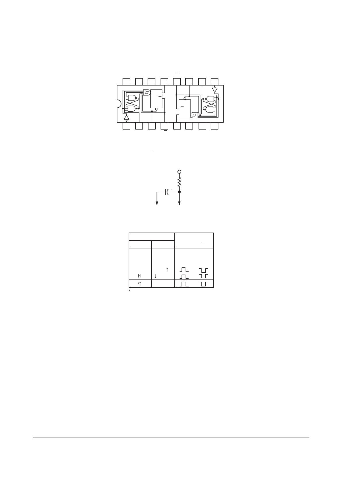
SN74LS221
http://onsemi.com
2
(TOP VIEW)
Positive logic: Low input to clear resets Q low and
Positive logic: Q
high regardless of dc levels at A
Positive logic: or B inputs.
14 13 12 11 10 9
123456
7
16 15
8
V
CC
1A
1 R
ext/
C
ext
1
C
ext
1Q 2Q 2B
2
CLR
2A
1B 1
CLR
1Q
2Q 2
C
ext
2 R
ext
/
C
ext
GND
Q
Q
CLR
Q
Q
CLR
+
V
CC
R
ext
R/CC
ext
FUNCTION TABLE
(EACH MONOSTABLE)
INPUTS OUTPUTS
CLEAR A B Q Q
L X X L H
X H XL H
X X LL H
H L
°
H
±
H
*
°
L H
*See operational notes — Pulse Trigger Modes
TYPE
TYPICAL
POWER
MAXIMUM
OUTPUT PULSE
DISSIPATION LENGTH
SN74LS221 23 mW 70 s

SN74LS221
http://onsemi.com
3
OPERATIONAL NOTES
Once in the pulse trigger mode, the output pulse width is
determined by t
W
= R
extCext
In2, as long as R
ext
and C
ext
are
within their minimum and maximum valves and the duty
cycle is less than 50%. This pulse width is essentially
independent of VCC and temperature variations. Output
pulse widths varies typically no more than ±0.5% from
device to device.
If the duty cycle, defined as being 100
@
t
W
T
where T is the
period of the input pulse, rises above 50%, the output pulse
width will become shorter. If the duty cycle varies between
low and high valves, this causes the output pulse width to
vary in length, or jitter. To reduce jitter to a minimum, R
ext
should be as large as possible. (Jitter is independent of C
ext
).
With R
ext
= 100K, jitter is not appreciable until the duty
cycle approaches 90%.
Although the LS221 is pin-for-pin compatible with the
LS123, it should be remembered that they are not
functionally identical. The LS123 is retriggerable so that the
output is dependent upon the input transitions once it is high.
This is not the case for the LS221. Also note that it is
recommended to externally ground the LS123 C
ext
pin.
However, this cannot be done on the LS221.
The SN74LS221 is a dual, monolithic, non-retriggerable,
high-stability one shot. The output pulse width, t
W
can be
varied over 9 decades of timing by proper selection of the
external timing components, R
ext
and C
ext
.
Pulse triggering occurs at a voltage level and is, therefore,
independent of the input slew rate. Although all three inputs
have this Schmitt-trigger effect, only the B input should be
used for very long transition triggers (≥1.0 µV/s). High
immunity to V
CC
noise (typically 1.5 V) is achieved by
internal latching circuitry. However, standard V
CC
bypassing is strongly recommended.
The LS221 has four basic modes of operation.
Clear Mode: If the clear input is held low, irregardless of
the previous output state and other input
states, the Q output is low.
Inhibit Mode:
If either the A input is high or the B input is
low, once the Q output goes low, it cannot
be retriggered by other inputs.
Pulse Trigger
Mode: A transition of the A or B inputs as indicated
in the functional truth table will trigger the Q
output to go high for a duration determined
by the t
W
equation described above; Q will
go low for a corresponding length of time.
The Clear input may also be used to trigger
an output pulse, but special logic preconditioning on the A or B inputs must be done
as follows:
Following any output triggering action
using the A or B inputs, the A input must
be set high OR the B input must be set
low to allow Clear to be used as a trigger.
Inputs should then be set up per the truth
table (without triggering the output) to
allow Clear to be used a trigger for the
output pulse.
If the Clear pin is routinely being used to
trigger the output pulse, the A or B inputs
must be toggled as described above
before and between each Clear trigger
event.
Once triggered, as long as the output
remains high, all input transitions (except
overriding Clear) are ignored.
Overriding
Clear Mode: If the Q output is high, it may be forced low
by bringing the clear input low.

SN74LS221
http://onsemi.com
4
DC CHARACTERISTICS OVER OPERATING TEMPERATURE RANGE (unless otherwise specified)
Limits
Symbol Parameter
Min Typ Max
Unit Test Conditions
V
T+
Positive-Going Threshold
Voltage at C Input
1.0 2.0 V VCC = MIN
V
T–
Negative-Going Threshold
Voltage at C Input
0.7 0.8 V
VCC = MIN
V
T+
Positive-Going Threshold
Voltage at B Input
1.0 2.0 V VCC = MIN
V
T–
Negative-Going Threshold
Voltage at B Input
0.8 0.9 V
VCC = MIN
V
IH
Input HIGH Voltage 2.0 V
Guaranteed Input HIGH Voltage for
A Input
V
IL
Input LOW Voltage
0.8
V
Guaranteed Input LOW Voltage for
A Input
V
IK
Input Clamp Voltage –1.5 V VCC = MIN, IIN = –18 mA
V
OH
Output HIGH Voltage 2.7 3.4 V VCC = MIN, IOH = MAX
V
OL
Output LOW Voltage 0.35 0.5 V IOL = 8.0 mA VCC = MIN
p
20 µA VCC = MAX, VIN = 2.7 V
IIHInput HIGH Current
0.1 mA VCC = MAX, VIN = 7.0 V
I
IL
Input LOW Current
Input A
Input B
Clear
–0.4
–0.8
–0.8
mA VCC = MAX, VIN = 0.4 V
I
OS
Short Circuit Current (Note 1) –20 –100 mA VCC = MAX
I
CC
Power Supply Current
Quiescent
4.7 11
mA VCC = MAX
CC
Triggered 19 27
CC
Note 1: Not more than one output should be shorted at a time, nor for more than 1 second.

SN74LS221
http://onsemi.com
5
AC CHARACTERISTICS (V
CC
= 5.0 V, TA = 25°C)
Limits
Symbol
From
(Input)
To
(Output)
Min Typ Max
Unit Test Conditions
A Q 45 70
t
PLH
B Q 35 55
ns
A Q 50 80
p
t
PHL
B Q 40 65
ns
C
ext
= 80 pF,
R
ext
= 2.0
Ω
t
PHL
Clear Q 35 55 ns
CL = 15 pF,
t
PLH
Clear Q 44 65 ns
L
See Figure 1
70 120 150 C
ext
= 80 pF, R
ext
= 2.0 Ω
20 47 70
ns
C
ext
= 0, R
ext
= 2.0 kΩ
t
W(out)
A or B
Q or Q
600 670 750 C
ext
= 100 pF, R
ext
= 10 kΩ
6.0 6.9 7.5 ms C
ext
= 1.0 µF, R
ext
= 10 kΩ
AC SETUP REQUIREMENTS (V
CC
= 5.0 V, TA = 25°C)
Limits
Symbol Parameter
Min Typ Max
Unit
Rate of Rise or Fall of Input Pulse
dv/dt
Schmitt, B 1.0 V/s
Logic Input, A 1.0 V/µs
Input Pulse Width
t
W
A or B, t
W(in)
40 ns
W
Clear, t
W
(clear) 40
t
s
Clear-Inactive-State Setup Time 15 ns
R
ext
External Timing Resistance 1.4 100 kΩ
C
ext
External Timing Capacitance 0 1000 µF
Output Duty Cycle
RT = 2.0 kΩ 50 %
RT = MAX R
ext
90

SN74LS221
http://onsemi.com
6
AC WAVEFORMS
B INPUT
CLEAR
Q OUTPUT
Q OUTPUT
A INPUT IS LOW.
B INPUT
CLEAR
Q OUTPUT
A INPUT IS LOW.
B INPUT
CLEAR
Q OUTPUT
A INPUT IS LOW.
t
W(in)
≥60 ns
t
PLH
t
PHL
t
PLH
t
PHL
1.3 V
3 V
0 V
3 V
0 V
V
OH
V
OL
V
OH
V
OL
≥60 ns
1.3 V
1.3 V
3 V
0 V
3 V
0 V
V
OH
V
OL
≥ 50 ns
≥ 0
t
s
3 V
0 V
3 V
0 V
V
OH
V
OL
3 V
0 V
3 V
0 V
V
OH
V
OL
TRIGGERED
NOT TRIGGERED
≥50 ns≥50 ns
B INPUT
CLEAR
Q OUTPUT
A INPUT IS LOW.
t
W(out)
TRIGGER FROM B, THEN CLEAR — CONDITION 1
TRIGGER FROM B, THEN CLEAR — CONDITION 2
CLEAR OVERRIDING B, THEN TRIGGER FROM B
TRIGGERING FROM POSITIVE TRANSITION OF CLEAR
Figure 1.

SN74LS221
http://onsemi.com
7
P ACKAGE DIMENSIONS
N SUFFIX
PLASTIC PACKAGE
CASE 648–08
ISSUE R
NOTES:
1. DIMENSIONING AND TOLERANCING PER ANSI
Y14.5M, 1982.
2. CONTROLLING DIMENSION: INCH.
3. DIMENSION L TO CENTER OF LEADS WHEN
FORMED PARALLEL.
4. DIMENSION B DOES NOT INCLUDE MOLD FLASH.
5. ROUNDED CORNERS OPTIONAL.
–A–
B
F
C
S
H
G
D
J
L
M
16 PL
SEATING
18
916
K
PLANE
–T–
M
A
M
0.25 (0.010) T
DIM MIN MAX MIN MAX
MILLIMETERSINCHES
A 0.740 0.770 18.80 19.55
B 0.250 0.270 6.35 6.85
C 0.145 0.175 3.69 4.44
D 0.015 0.021 0.39 0.53
F 0.040 0.70 1.02 1.77
G 0.100 BSC 2.54 BSC
H 0.050 BSC 1.27 BSC
J 0.008 0.015 0.21 0.38
K 0.110 0.130 2.80 3.30
L 0.295 0.305 7.50 7.74
M 0 10 0 10
S 0.020 0.040 0.51 1.01
____
D SUFFIX
PLASTIC SOIC PACKAGE
CASE 751B–05
ISSUE J
NOTES:
1. DIMENSIONING AND TOLERANCING PER ANSI
Y14.5M, 1982.
2. CONTROLLING DIMENSION: MILLIMETER.
3. DIMENSIONS A AND B DO NOT INCLUDE
MOLD PROTRUSION.
4. MAXIMUM MOLD PROTRUSION 0.15 (0.006)
PER SIDE.
5. DIMENSION D DOES NOT INCLUDE DAMBAR
PROTRUSION. ALLOWABLE DAMBAR
PROTRUSION SHALL BE 0.127 (0.005) TOTAL
IN EXCESS OF THE D DIMENSION AT
MAXIMUM MATERIAL CONDITION.
18
16 9
SEATING
PLANE
F
J
M
R
X 45
_
G
8 PLP
–B–
–A–
M
0.25 (0.010) B
S
–T–
D
K
C
16 PL
S
B
M
0.25 (0.010) A
S
T
DIM MIN MAX MIN MAX
INCHESMILLIMETERS
A 9.80 10.00 0.386 0.393
B 3.80 4.00 0.150 0.157
C 1.35 1.75 0.054 0.068
D 0.35 0.49 0.014 0.019
F 0.40 1.25 0.016 0.049
G 1.27 BSC 0.050 BSC
J 0.19 0.25 0.008 0.009
K 0.10 0.25 0.004 0.009
M 0 7 0 7
P 5.80 6.20 0.229 0.244
R 0.25 0.50 0.010 0.019
____

SN74LS221
http://onsemi.com
8
ON Semiconductor and are trademarks of Semiconductor Components Industries, LLC (SCILLC). SCILLC reserves the right to make changes
without further notice to any products herein. SCILLC makes no warranty , representation or guarantee regarding the suitability of its products for any particular
purpose, nor does SCILLC assume any liability arising out of the application or use of any product or circuit, and specifically disclaims any and all liability ,
including without limitation special, consequential or incidental damages. “Typical” parameters which may be provided in SCILLC data sheets and/or
specifications can and do vary in different applications and actual performance may vary over time. All operating parameters, including “Typicals” must be
validated for each customer application by customer’s technical experts. SCILLC does not convey any license under its patent rights nor the rights of others.
SCILLC products are not designed, intended, or authorized for use as components in systems intended for surgical implant into the body, or other applications
intended to support or sustain life, or for any other application in which the failure of the SCILLC product could create a situation where personal injury or
death may occur. Should Buyer purchase or use SCILLC products for any such unintended or unauthorized application, Buyer shall indemnify and hold
SCILLC and its officers, employees, subsidiaries, affiliates, and distributors harmless against all claims, costs, damages, and expenses, and reasonable
attorney fees arising out of, directly or indirectly , any claim of personal injury or death associated with such unintended or unauthorized use, even if such claim
alleges that SCILLC was negligent regarding the design or manufacture of the part. SCILLC is an Equal Opportunity/Affirmative Action Employer .
PUBLICATION ORDERING INFORMATION
ASIA/PACIFIC: LDC for ON Semiconductor – Asia Support
Phone: 303–675–2121 (Tue–Fri 9:00am to 1:00pm, Hong Kong Time)
T oll Free from Hong Kong 800–4422–3781
Email: ONlit–asia@hibbertco.com
JAPAN: ON Semiconductor, Japan Customer Focus Center
4–32–1 Nishi–Gotanda, Shinagawa–ku, T okyo, Japan 141–8549
Phone: 81–3–5487–8345
Email: r14153@onsemi.com
Fax Response Line: 303–675–2167
800–344–3810 Toll Free USA/Canada
ON Semiconductor Website: http://onsemi.com
For additional information, please contact your local
Sales Representative.
SN74LS221/D
North America Literature Fulfillment:
Literature Distribution Center for ON Semiconductor
P.O. Box 5163, Denver, Colorado 80217 USA
Phone: 303–675–2175 or 800–344–3860 T oll Free USA/Canada
Fax: 303–675–2176 or 800–344–3867 Toll Free USA/Canada
Email: ONlit@hibbertco.com
N. American Technical Support: 800–282–9855 Toll Free USA/Canada
EUROPE: LDC for ON Semiconductor – European Support
German Phone: (+1) 303–308–7140 (M–F 2:30pm to 5:00pm Munich Time)
Email: ONlit–german@hibbertco.com
French Phone: (+1) 303–308–7141 (M–F 2:30pm to 5:00pm Toulouse Time)
Email: ONlit–french@hibbertco.com
English Phone: (+1) 303–308–7142 (M–F 1:30pm to 5:00pm UK Time)
Email: ONlit@hibbertco.com
 Loading...