

Motorola PZTA42T1 Datasheet
1
Motorola Small–Signal Transistors, FETs and Diodes Device Data
NPN Silicon
MAXIMUM RATINGS
Rating Symbol Value Unit
Collector-Emitter Voltage (Open Base) V
CEO
300 Vdc
Collector-Base Voltage (Open Emitter) V
CBO
300 Vdc
Emitter-Base Voltage (Open Collector) V
EBO
6.0 Vdc
Collector Current (DC) I
C
500 mAdc
Total Power Dissipation @ TA = 25°C
(1)
P
D
1.5 Watts
Storage Temperature Range T
stg
–65 to +150 °C
Junction Temperature T
J
150 °C
DEVICE MARKING
P1D
THERMAL CHARACTERISTICS
Characteristic Symbol Max Unit
Thermal Resistance,
Junction-to-Ambient
(1)
R
θJA
83.3 °C/W
ELECTRICAL CHARACTERISTICS (T
A
= 25°C unless otherwise noted)
Characteristics
Symbol Min Max Unit
OFF CHARACTERISTICS
Collector-Emitter Breakdown Voltage
(2)
(IC = 1.0 mAdc, IB = 0)
V
(BR)CEO
300 — Vdc
Collector-Base Breakdown Voltage
(IC = 100 µAdc, IE = 0)
V
(BR)CBO
300 — Vdc
Emitter-Base Breakdown Voltage
(IE = 100 µAdc, IC = 0)
V
(BR)EBO
6.0 — Vdc
Collector-Base Cutoff Current
(VCB = 200 Vdc, IE = 0)
I
CBO
— 0.1 µAdc
Emitter-Base Cutoff Current
(VBE = 6.0 Vdc, IC = 0)
I
EBO
— 0.1 µAdc
1. Device mounted on a glass epoxy printed circuit board 1.575 in. x 1.575 in. x 0.059 in.; mounting pad for the collector lead min 0.93 in2.
2. Pulse Test Conditions, tp = 300 µs, δ = 0.02.
Thermal Clad is a trademark of the Bergquist Company
Preferred devices are Motorola recommended choices for future use and best overall value.
Order this document
by PZTA42T1/D
SEMICONDUCTOR TECHNICAL DATA
Motorola, Inc. 1996
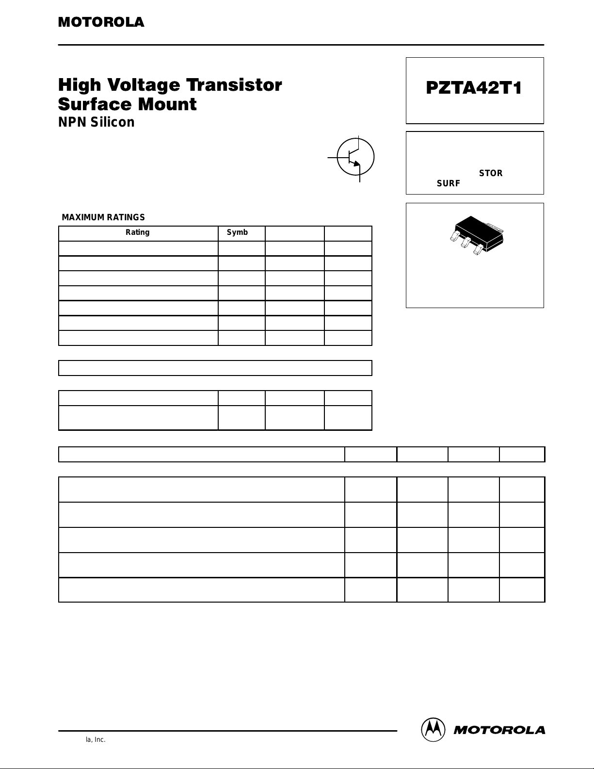
SOT–223 PACKAGE
NPN SILICON
HIGH VOLTAGE
TRANSISTOR
SURFACE MOUNT
Motorola Preferred Device
CASE 318E-04, STYLE 1
TO-261AA
1
2
3
4
COLLECTOR 2,4
BASE
1
EMITTER 3
REV 2
PZTA42T1
2
Motorola Small–Signal Transistors, FETs and Diodes Device Data
ELECTRICAL CHARACTERISTICS
(T
A
= 25°C unless otherwise noted) (Continued)
ON CHARACTERISTICS
DC Current Gain
(IC = 1.0 mAdc, VCE = 10 Vdc)
(IC = 10 mAdc, VCE = 10 Vdc)
(IC = 30 mAdc, VCE = 10 Vdc)
h
FE
25
40
40
—
—
—
—
DYNAMIC CHARACTERISTICS
Current-Gain — Bandwidth Product
(IC = 10 mAdc, VCE = 20 Vdc, f = 100 MHz)
f
T
50 — MHz
Feedback Capacitance
(VCB = 20 Vdc, IE = 0, f = 1.0 MHz)
C
re
— 3.0 pF
Collector-Emitter Saturation Voltage
(IC = 20 mAdc, IB = 2.0 mAdc)
V
CE(sat)
— 0.5 Vdc
Base-Emitter Saturation Voltage
(IC = 20 mAdc, IB = 2.0 mAdc)
V
BE(sat)
— 0.9 Vdc
 Loading...