

Motorola PZTA14T1 Datasheet
1
Motorola Small–Signal Transistors, FETs and Diodes Device Data
This NPN small signal darlington transistor is designed for use in switching
applications, such as print hammer, relay, solenoid and lamp drivers. The
device is housed in the SOT -223 package, which is designed for medium power
surface mount applications.
• High fT: 125 MHz Minimum
• The SOT-223 Package can be soldered using wave or reflow.
• SOT-223 package ensures level mounting, resulting in improved thermal
conduction, and allows visual inspection of soldered joints. The formed
leads absorb thermal stress during soldering, eliminating the possibility of
damage to the die.
• Available in 12 mm Tape and Reel
Use PZTA14T1 to order the 7 inch/1000 unit reel
Use PZTA14T3 to order the 13 inch/4000 unit reel
• The PNP Complement is PZTA64T1
MAXIMUM RATINGS
(T
C
= 25°C unless otherwise noted)
Rating
Symbol Value Unit
Collector-Emitter Voltage V
CES
30 Vdc
Collector-Emitter Voltage V
CEO
30 Vdc
Emitter-Base Voltage V
EBO
10 Vdc
Collector Current I
C
300 mAdc
Total Power Dissipation @ TA = 25°C
(1)
P
D
1.5 Watts
Operating and Storage Temperature Range TJ, T
stg
–65 to 150 °C
DEVICE MARKING
P1N
THERMAL CHARACTERISTICS
Thermal Resistance
Junction-to-Ambient (surface mounted)
R
θJA
83.3 °C/W
Maximum Temperature for Soldering Purposes
Time in Solder Bath
T
L
260
10
°C
Sec
1. Device mounted on a FR-4 glass epoxy printed circuit board 1.575 in. x 1.575 in. x 0.0625 in.; mounting pad for the collector lead = 0.93 sq. in.
Thermal Clad is a trademark of the Bergquist Company
Preferred devices are Motorola recommended choices for future use and best overall value.
Order this document
by PZTA14T1/D
SEMICONDUCTOR TECHNICAL DATA
Motorola, Inc. 1996
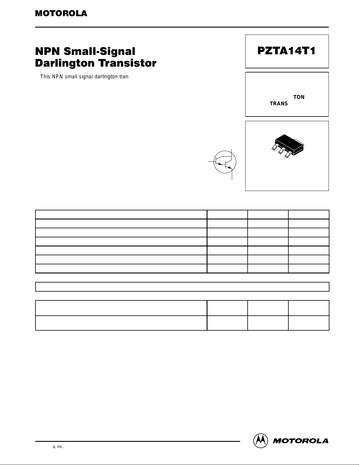
SOT–223 PACKAGE
MEDIUM POWER
NPN SILICON
DARLINGTON
TRANSISTOR
SURFACE MOUNT
Motorola Preferred Device
CASE 318E-04, STYLE 1
TO-261AA
1
2
3
4
COLLECTOR 2, 4
BASE
1
EMITTER 3
REV 1
PZTA14T1
2
Motorola Small–Signal Transistors, FETs and Diodes Device Data
ELECTRICAL CHARACTERISTICS
(T
A
= 25°C unless otherwise noted)
Characteristics
Symbol Min Typ Max Unit
OFF CHARACTERISTICS
Collector-Base Breakdown Voltage
(IC = 100 µAdc, IE = 0)
V
(BR)CBO
30 — — Vdc
Collector-Emitter Breakdown Voltage
(IC = 100 µAdc, IB = 0)
V
(BR)CES
30 — — Vdc
Emitter-Base Breakdown Voltage
(IE = 10 µAdc, IC = 0)
V
(BR)EBO
10 — — Vdc
Collector-Base Cutoff Current
(VCB = 30 Vdc, IE = 0)
I
CBO
— — 0.1 µAdc
Emitter-Base Cutoff Current
(VEB = 10 Vdc, IC = 0)
I
EBO
— — 0.1 µAdc
ON CHARACTERISTICS (2)
DC Current Gain
(IC = 10 mAdc, VCE = 5.0 Vdc)
(IC = 100 mAdc, VCE = 5.0 Vdc)
h
FE
10,000
20,000
—
—
—
—
—
Collector-Emitter Saturation Voltage
(IC = 100 mAdc, IB = 0.1 mAdc)
V
CE(sat)
— — 1.5 Vdc
Base-Emitter On Voltage
(IC = 100 mAdc, VCE = 5.0 Vdc)
V
BE(on)
— — 2.0 Vdc
DYNAMIC CHARACTERISTICS
Current-Gain — Bandwidth Product
(IC = 10 mAdc, VCE = 5.0 Vdc)
f
T
125 — — MHz
2. Pulse Test: Pulse Width ≤ 300 µs, Duty Cycle ≤ 2.0%.
 Loading...