How it Works
Log In / Sign Up
Buy Points
How it Works
FAQ
Contact Us
Questions and Suggestions
Users
Motorola
Loading...
M
MVME2700-43X1
MVME2700-4421
MVME2700-4461
MVME2700-44X1
MVME3100
2
MVME3600
MVME4600
MVME5100
5
MVME5500
2
MVME55006E
MVME6100
2
MVME6100-0161
MVME6100-0163
MVME6100-0171
MVME6100-0173
MVME712-10
MVME712-12
MVME712-13
2
MVME712A
2
MVME712A-D3
2
MVME712AM
2
MVME712B
2
MVME712M
MVME760
MVME761-001
MVME761-011
MVME956AC
MVME956UM2
MVMEl36A
mVoiceMail v5.0.1
MVX1000
MW800
3
MW810
3
MWR6300
MWR815
MWR839
MX101
MX1200
MX240A
MX300
3
MX300-S
MX320
MX330
MX330-S
MX340
MX340-S
MX350
MX350-S
MX360
MX360-S
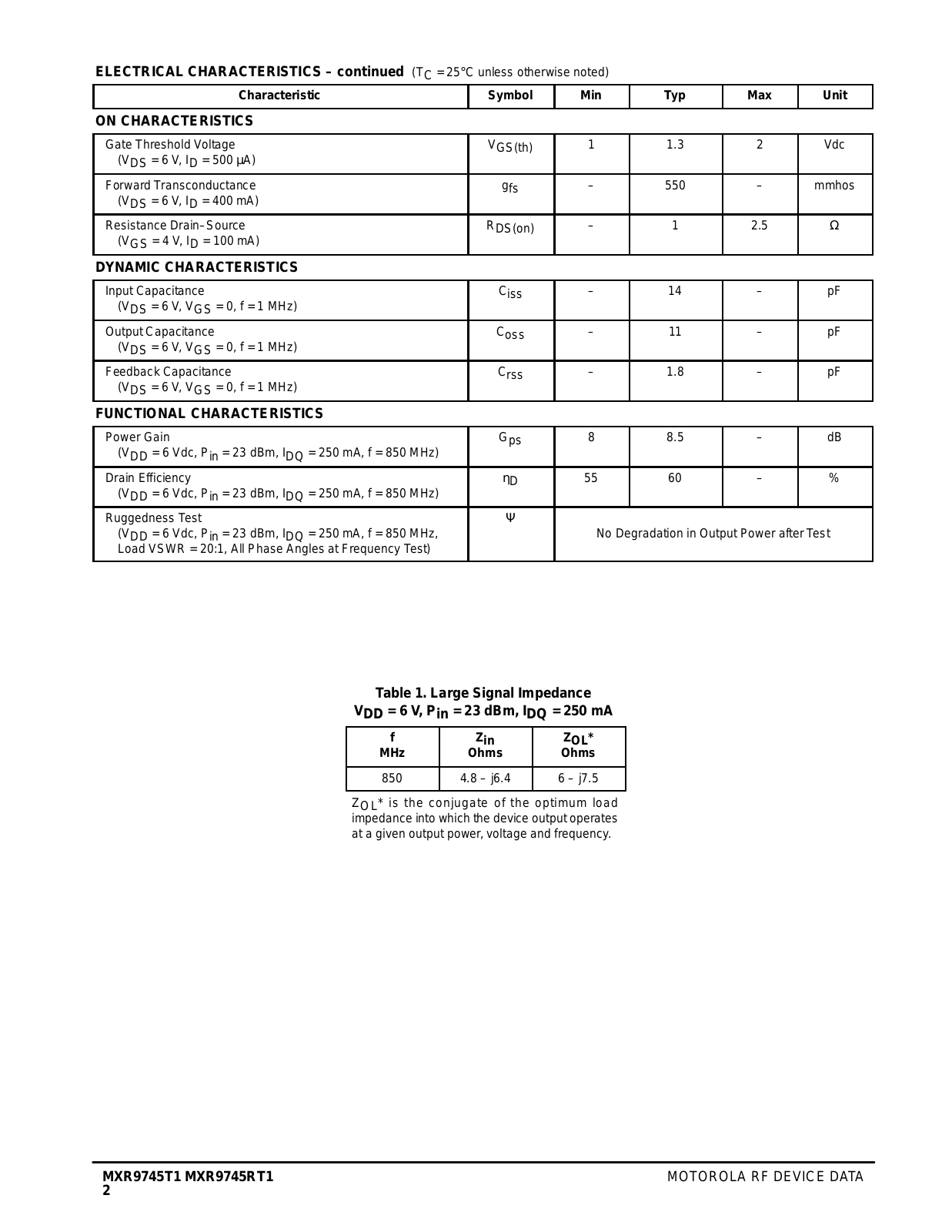
MXR9745RT1
MXR9745T1
MXV3
MXV4 IR
MXv5 IR
MZ505
MZ601
4
MZ606
2
MZ607
MZ608
MZ615-16
MZ616
MZP4728
MZPY100RL
MZPY10RL
MZPY11RL
MZPY12RL
MZPY13RL
MZPY15RL
MZPY16RL
MZPY18RL
MZPY22RL
MZPY24RL
MZPY27RL
MZPY30RL
MZPY33RL
MZPY36RL
MZPY3.9RL
MZPY4.3RL
MZPY4.7RL
MZPY5.1RL
MZPY56RL
MZPY6.2RL
MZPY6.8RL
MZPY7.5RL
MZPY8.2RL
MZPY9.1RL
N
NA7004
NC800
NCP1205P
NCP1205P2
NCP1232DR2
NCP1560HDR2
NCP566
NCP5663
NCP566ST25T3G
NCS6416
NCS6416DWG
NCT47SNT1
NCV5663DS15R4G
Loading...
Loading...
Nothing found
MXR9745RT1
Datasheet
4 pgs
54.67 Kb
0
Table of contents
Loading...
Motorola MXR9745RT1, MXR9745T1 Datasheet
...
Motorola Datasheet
Download
Specifications and Main Features
Frequently Asked Questions
User Manual
Download
Loading...
+
2
hidden pages
Unhide
You need points to download manuals.
1 point = 1 manual.
You can buy points or you can get point for every manual you upload.
Buy points
Upload your manuals
 Loading...