

Page 1

MVME5100
Single Board Computer
Installation an d Use
V5100A/IH4
July 2003 Edition
Page 2

© Copyright 2003 Motorola, Inc.
All rights reserved.
Printed in the United States of America.
Motorola and the Motorola logo are registered trademarks and AltiVec is a trademark of
Motorola, Inc.
PowerPC and the PowerPC logo are registered trademarks; and PowerPC 750 is a
trademark of International Business Machines Corporation and are used by Motorola, Inc.
under license from International Business Machines Corporation.
All other products mentioned in this document are tr ade ma rks or re gi st ered trademarks of
their respective holders.
Page 3

Safety Summary
The following general safety precautions must be observed during all phases of operation, service, and repair of this
equipment. Failure to comply with these precautions or with specific warnings elsewhere in this manual could result
in personal injury or damage to the equipment.
The safety preca utions listed be low represent warnings o f certain danger s of which M otorola is awar e. You, as the
user of the product, should follow these warnings and all other safety precautions necessary for the safe operation of
the equipment in your operating envir onment.
Ground the Instrument.
To minimize shock hazard, the equipment chassis and enclosure must be connected to an electrical ground. If the
equipment is su pplied with a three-c onductor AC power ca ble, the pow er cable mus t be plugg ed into an a pproved
three-contact electrical o utlet, with the grounding wire (green/yellow) reliably connected to an electrical ground
(safety ground) at the power outlet. The power jack and mating plug of the power cable meet International
Electrotechnical C om mission (IEC) sa fety standards and lo cal electrical regulat or y codes.
Do Not Operate in an Explosive Atmosphere.
Do not operate the equipment in any explosive atmosphere such as in the presence of flammable gases or fumes.
Operation of any electrical equipment in such an environment could result in an explosion and cause injury or damage.
Keep Away From Live Circuits Inside the Equipment.
Operating personnel must not remove equipment covers. Only Factory Authorized Service Personnel or other
qualified service personnel may remove equipment covers for internal subassembly or component replacement or any
internal adjust ment. Service pe rsonnel should n ot replace compon ents with power c able connected. Under certain
conditions, dangerous voltages may exist even with th e power cable removed. To avoid injuries, such personnel
should always disconnect power and discharge circuits bef or e touching component s.
Use Caution When Exposing or Handling a CRT.
Breakage of a Cathode-Ray Tube (CRT) causes a high-velocity scattering of glass fragments (implosion). To prevent
CRT implosion, do not handle t he CRT and avoid rough handling or jarring of the equipment. Handling of a CRT
should be done only by qualified service personnel using approved safety mask and gloves.
Do Not Substitute Parts or Modify Equipment.
Do not install substitute parts or perform any unauthorized modification of the equipment. Contact your local
Motorola representative for service and repair to ensure that all safety features are maintained.
Observe Warnings in Manual.
W arning s, such as th e example belo w, precede potentially dangerous procedures through out this ma nual. In structio ns
contained in the w arnings mu st be followe d. You should also employ all othe r safety pr ecautions wh ich you deem
necessary for the operation of the equipment in your operating environme nt .
To prevent serious injury or death from dangerous voltages, use extreme
caution when handling, testing, and adjusting this equipment and its
Warning
components.
Page 4

Flammability
All Motorola PWBs (printed wiring boar ds) are manufactured with a flammabilit y rating
of 94V-0 by UL-recognized manufacturers.
EMI Caution
This equipment ge nerat es, us es and can r adiat e el ectro magneti c ene rgy . It
!
Caution
This product contains a lithium battery to power the clock and calendar circuitry.
!
Caution
may cause or be susceptible to electromagnetic interference (EMI) if not
installed and used with adequate EMI protection.
Lithium Battery Caution
Danger of explosion if battery is repl aced incorrectly. Replace battery only
with the same or equivalent type recommended by the equipment
manufacturer. Dispose of used batteries according to the manufacturer’s
instructions.
!
Attention
!
Vorsicht
Il y a danger d’explosion s’il y a remplacement incorrect de la batterie.
Remplacer uniquement avec une batterie du même type ou d’un type
équivalent recommandé par le constructeur. Mettre au rebut les batteries
usagées conformément aux instructions du fabricant.
Explosionsgefahr b ei uns achg emäßem Austausch der Batt er ie . Ers at z nur
durch denselben ode r einen vom Herstel ler empfohle nen Typ. Entsorgu ng
gebrauchter Batterien nach Angaben des Herstellers.
Page 5

CE Notice (European Community)
Motorola Computer Gr oup product s with the CE marking co mply with the EMC Dir ective
(89/336/EEC). Compliance with this directive implies conformity to the following
European Norms:
EN55022 “Limits and Methods of Measur ement of Ra dio Int erferen ce Chara cteri stic s
of Information Technology Equipment”; this product tested to Equipment Class B
EN55024 “Information te chnology equipment—Immunity c haracteristics—Limits an d
methods of measurement”
Board products are tested in a representative system to show compliance with the above
mentioned requirements. A proper installation in a CE-marked system will maintain the
required EMC performance.
In accordance with European Community directives, a “Declaration of Conformity” has
been made and is available on request. Please contact your sales representative.
Notice
While reasonable efforts have been made to assure the accuracy of this document,
Motorola, Inc. a ssumes n o liabil ity res ulting f rom any omissions in thi s document, or fr om
the use of the information obtained therein. Motorola reserves the ri ght to revise this
document and to make c hanges from time to time in the content hereof without obliga ti on
of Motorola to notify any person of such revision or changes.
Electronic versions of this material may be read online, downloaded for personal use, or
referenced in another document as a URL to the Motorola Computer Group website. The
text itself may n ot be published co mmercially in p rint or electroni c form, edited, tr anslated,
or otherwise altered without the permission of Motorola, Inc.
It is possible that this publication may contain reference to or information about Motorola
products (machines and pr ograms), progra mming, or servi ces that are not av ailable in yo ur
country. Such references or information must not be construed to mean that Motorola
intends to announce such Motorola products, programming, or services in your country.
Page 6

Limited and Restricted Rights Legend
If the documentation contained herein is supplied, directly or indirectly, to the U.S.
Government, the following notice shall apply unless otherwise agreed to in writing by
Motorola, Inc.
Use, duplication, or disclosure by the Government is subject to restrictions as set forth in
subparagraph (b)(3) of the Rights in Technical Data clause at DFARS 252.227-7013
(Nov. 1995) and of the Rights in Noncommercial Computer Software and Documentation
clause at DFARS 252.227-7014 (Jun. 1995).
Motorola, Inc.
Computer Group
2900 South Diablo Way
Tempe, Arizona 85282
Page 7

Contents
About This Manual
Summary of Changes................................................................................................xvii
Overview of Contents...............................................................................................xvii
Comments and Suggestions.......................................................................................xix
Conventions Used in This Manual.............................................................................xix
Terminology.........................................................................................................xx
CHAPTER 1 Hardware Preparation and Installation
Introduction ................................................................................................................1-1
Getting Started ............................................................................... ...... ..... .................1-1
Overview and Equipment Requirements............................................................1-1
Unpacking Instructions.......................................................................................1-2
Preparation.................................................................................................................1-3
Hardware Configuration.....................................................................................1-3
Jumper Settings...................................................................................................1-5
PMC/SBC (761/IPMC) Mode Selection.....................................................1-6
Installation Considerations ............................................... ..................................1-6
Installation..................................................................................................................1-8
PMC Modules...................................................................................................1-10
Primary PMCspan.............................................................................................1-12
Secondary PMCspan.........................................................................................1-14
MVME5100......................................................................................................1-16
CHAPTER 2 Operation
Introduction ................................................................................................................2-1
Switches and Indicators ........................................................... ...... ...... ......................2-1
ABT/RST Switch................................................................................................2-1
Abort Function.............................................................................................2-1
Reset Function.............................................................................................2-1
Status Indicators..................................................................................................2-2
RST Indicator (DS1).................................................. ...... ...... ......................2-2
CPU Indicator (DS2)...................................................................................2-2
Connectors..........................................................................................................2-2
10/100 BASE T Ports..................................................................................2-3
vii
Page 8

DEBUG Port ............................................................ .................................. .2-3
System Powerup........................................................................................................2-3
Initialization Process ..........................................................................................2-4
CHAPTER 3 PPCBug Firmware
Introduction ...............................................................................................................3-1
PPCBug Overview.....................................................................................................3-1
Implementation and Memory Requirements......................................................3-3
Using PPCBug........................................................................................................... 3-3
Hardware and Firmware Initialization ...............................................................3-4
Default Settings ............................................... ...... .................................. ..... ...... .......3-6
CNFG - Configure Board Information Block ....................................................3-7
ENV - Set Environment .....................................................................................3-7
Configuring the PPCBug Parameters..........................................................3-8
LED/Serial Startup Diagnostic Codes..............................................................3-16
Configuring the VMEbus Interface.................................................................. 3-17
Firmware Command Buffer ............................................ ..... ...... ......................3-21
Standard Commands................................................................................................3-22
Diagnostics....................................................................................................... 3-26
CHAPTER 4 Functional Description
Introduction ...............................................................................................................4-1
Features Summary..................................................................................................... 4-1
Features Descriptions ................................................................................................ 4-3
General ...............................................................................................................4-3
Processor ............................................................................................................ 4-5
System Memory Controller and PCI Host Bridge..............................................4-5
Memory..............................................................................................................4-5
Flash Memory .............................................................................................4-5
ECC SDRAM Memory...............................................................................4-6
P2 Input/Output (I/O) Modes.............................................................................4-7
Input/Output Interfaces.......................................................................................4-7
Ethernet Interface........................................................................................4-7
VMEbus Interface....................... .................................. ...... ...... .................. 4-8
Asynchronous Communications.................................................................4-8
Real-Time Clock & NVRAM & Watchdog Timer.....................................4-8
Timers .........................................................................................................4-8
Interrupt Routing.........................................................................................4-8
IDSEL Routing............................................................................................4-9
viii
Page 9

CHAPTER 5 Pin Assignments
Introduction ................................................................................................................5-1
Summary.............................................................................................................5-1
Jumper Settings..........................................................................................................5-2
Connectors .................................................................................................................5-3
IPMC761 Connector (J3) Pin Assignments........................................................5-3
Memory Expansion Connector (J8) Pin Assignments........................................5-4
PCI Expansion Connector (J25) Pin Assignments .............................................5-7
PCI Mezzanine Card (PMC) Connectors..........................................................5-10
VMEbus Connectors P1 & P2 Pin Assignments (PMC mode)........................5-23
VMEbus P1 & P2 Connector Pin Assignments (SBC Mode)..........................5-25
10 BaseT/100 BaseTx Connector Pin Assignments.........................................5-29
COM1 and COM2 Connector Pin Assignments...............................................5-30
CHAPTER 6 Programming the MVME51xx
Introduction ................................................................................................................6-1
Memory Maps........................................ ...... .................................. ...... ......................6-1
Processor Bus Memory Map...............................................................................6-2
Default Processor Memory Map..................................................................6-2
Processor Memory Map........................................ .................................. .....6-3
PCI Memory Map........................................................................................6-5
VME Memory Map.....................................................................................6-5
PCI Local Bus Memory Map..............................................................................6-5
VMEbus Memory Map.......................................... .................................. ...... .....6-6
Programming Considerations.....................................................................................6-6
PCI Arbitration ...................................................................................................6-6
Interrupt Handling...............................................................................................6-9
DMA Channels.................................................................................................6-11
Sources of Reset................................................................................................6-11
Endian Issues....................................................................................................6-13
Processor/Memory Domain....................................... ................................6-13
PCI Domain...............................................................................................6-13
VMEbus Domain............................................ ...........................................6-14
APPENDIX A Specifications
General Specifications ..............................................................................................A-1
Power Requirements......................... ........................................................................A-2
Cooling Requirements ..............................................................................................A-3
ix
Page 10

EMC Compliance.....................................................................................................A-3
APPENDIX B Troubleshooting
Solving Startup Problems.........................................................................................B-1
APPENDIX C Related Documentation
Motorola Computer Group Documents.................................................................... C-1
Manufacturers’ Documents...................................................................................... C-2
Related Specifications .............................................................................................. C-4
APPENDIX D RAM500 Memory Expansion Module
Overview ..................................................................................................................D-1
Features.....................................................................................................................D-1
Functional Description .............................................................................................D-2
RAM500 Description........................................................................................D-2
SROM................................................................................................................D-5
Host Clock Logic...............................................................................................D-5
RAM500 Module Installation...................................................................................D-5
RAM500 Connectors................................................................................................D-7
Bottom Side Memory Expansion Connector (P1).............................................D-7
Top Side Memory Expansion Connector (J1).................................................D-10
RAM500 Programming Issues...............................................................................D-13
Serial Presence Detect (SPD) Data .................................................................D-13
APPENDIX E Thermal Analysis
Thermally Significant Components...........................................................................E-1
Component Temperature Measurement.....................................................................E-6
Preparation..........................................................................................................E-6
Measuring Junction Temperature .......................................................................E-6
Measuring Case Temperature.............................................................................E-6
Measuring Local Air Temperature .....................................................................E-9
x
Page 11

List of Figures
Figure 1-1. MVME5100 Layout................................................................................1-9
Figure 1-2. MVME5100 Installation and Removal From a VMEbus Chassis........1-11
Figure 1-3. Typical PMC Module Placement on an MVME5100...........................1-11
Figure 1-4. PMCspan-002 Installation on an MVME510 .......................................1-13
Figure 1-5. PMCspan-010 Installation on a PMCspan-002/MVME5100 ...............1-15
Figure 2-1. Boot-Up Sequence ..................................................................................2-5
Figure 4-1. MVME5100 Block Diagram...................................................................4-4
Figure 6-1. VMEbus Master Mapping.......................................................................6-8
Figure 6-2. MVME510x Interrupt Architecture......................................................6-10
Figure D-1. RAM500 Block Diagram .....................................................................D-4
Figure D-2. RAM500 Module Placement on MVME5100 .....................................D-6
Figure E-1. Thermally Significant Components on the MVME5100 Single
Board Computer - Primary Side .............................................................................E-4
Figure E-2. Thermally Significant Components on the IPMC761 Module -
Primary Side .............................................................................................................E-5
Figure E-3. Mounting a Thermocouple Under a Heatsink .......................................E-8
Figure E-4. Measuring Local Air Temperature ....................................................... E-9
xi
Page 12

xii
Page 13

List of Tables
Table 1-1. Manually Configured Headers/Jumpers ...................................................1-4
T ab le 3-1. Debugger Command s.................................. ...... ..... ................................3-22
Table 3-2. Diagnostic Test Groups...........................................................................3-27
Table 4-1. MVME5100 General Features..................................................................4-1
Table 5-1. Jumper Switches and Settings...................................................................5-2
T ab le 5-2. IPMC761 Connector Pin Assignments.....................................................5-3
Table 5-3. Memory Expansion Connector Pin Assignments.....................................5-4
Table 5-4. PCI Expansion Connector
Pin Assignments.........................................................................................................5-7
Table 5-5. PMC Slot 1 Connector (J11) Pin Assignments.......................................5-10
Table 5-6. PMC Slot 1 Connector (J12) Pin Assignments.......................................5-12
Table 5-7. PMC Slot 1 Connector (J13) Pin Assignments.......................................5-13
Table 5-8. PMC Slot 1 Connector (J14)
Pin Assignments.......................................................................................................5-15
Table 5-9. PMC Slot 2 Connector (J21) Pin Assignments.......................................5-17
Table 5-10. PMC Slot 2 Connector (J22) Pin Assignments.....................................5-18
Table 5-11. PMC Slot 2 Connector (J23) Pin Assignments.....................................5-20
Table 5-12. PMC Slot 2 Connector (J24) Pin Assignments.....................................5-21
Table 5-13. VMEbus Connector P2 Pin Assignments
(PMC Mode)............................................................................................................5-23
Table 5-14. VMEbus P2 Connector Pinouts with IPMC761-
SBC Mode................................................................................................................5-25
Table 5-15. VMEbus Connector P2 Pinout with IPMC712 .....................................5-27
Table 5-16. 10 BaseT/100 BaseTx Connector Pin Assignment...............................5-29
Table 5-17. COM1 (J19) Connector Pin Assignments ............................................5-30
Table 5-18. COM2 (J5) Connector Pin Assignments ..............................................5-30
T ab le 6-1. Default Processor Memory Map...............................................................6-2
T ab le 6-2. Suggested CHRP Memory Map ...............................................................6-3
Table 6-3. Hawk PPC Register Values for Suggested Memory Map.........................6-4
T ab le 6-4. PCI Arbitration Assignments........................................ ...... ......................6-9
Table A-1. MVME5100 Specifications ...................................................................A-1
Table A-2. Power Consumption ..............................................................................A-2
Table B-1. Troubleshooting Problems .....................................................................B-1
Table C-1. Motorola Computer Group Documents .................................................C-1
Table C-2. Manufacturers’ Documents ....................................................................C-2
xiii
Page 14

Table C-3. Related Specifications ........................................................................... C-4
Table D-1. RAM500 Feature Summary ..................................................................D-1
Table D-2. RAM500 SDRAM Memory Size Options ............................................D-3
Table D-3. RAM500 Bottom Side Connector (P1)
Pin Assignments ......................................................................................................D-8
Table D-4. RAM500 Top Side Connector (J1)
Pin Assignments ....................................................................................................D-10
Table E-1. Thermally Significant Components on the MVME5100 Single
Board Computer .......................................................................................................E-2
Table E-2. Thermally Significant Components on the IPMC761 Module ..............E-3
xiv
Page 15

About This Manual
The MVME51xx Single Board Computer Installation and Use provides the
information you will need to install and configure your MVME51xx
Single Board Computer. It provides specific preparation and installation
information and data app licable to the board
The MVME51xx is a high-performance VME single board computer
featuring the Mo torola Computer Group (MCG) PowerPlus II arc hitecture
with a choice of proc essor s—either Motorol a’s MPC741 0 with AltiVec
technology for algorithmic intensive computations or the low-power
MPC755 or MPC750.
As of the printing date of th is man ual, the MVME51xx is available in the
configurations shown below. Note: all models of the MVME51xx are
available with either VME Scanbe front panel (-xxx) or IEEE 1101
compatible front panel (-xxx3) handles.
Part Number Description
450 MHz MPC750 Commercial Models
MVME5100-016x 450 MHz MPC750, 512MB ECC SDRAM, 17MB Flash and 1MB L2 cache
400 MHz MPC755 Extended Temperature Models
MVME5106-114x 400 MHz MPC755, 128MB ECC SDRAM, 17MB Flash and 1MB L2 cache
MVME5106-115x 400 MHz MPC755, 256MB ECC SDRAM, 17MB Flash and 1MB L2 cache
MVME5106-116x 400 MHz MPC755, 512MB ECC SDRAM, 17MB Flash and 1MB L2 cache
400 and 500 MHz MPC7410 Commercial Models
MVME5110-216x 40 0 MHz MPC7410, 512 MB ECC SDRAM, 17MB Flash and 2MB L2 cache
MVME5110-226x 50 0 MHz MPC7410, 512 MB ECC SDRAM, 17MB Flash and 2MB L2 cache
500 MHz MPC7410 Extended Temperature Models
MVME5107-214x 500 MHz MPC7410, 128MB ECC SDRAM, 17MB Flash and 2MB L2 cache
MVME5107-215x 500 MHz MPC7410, 256MB ECC SDRAM, 17MB Flash and 2MB L2 cache
MVME5107-216x 500 MHz MPC7410, 512MB ECC SDRAM, 17MB Flash and 2MB L2 cache
MVME712M Compatible I/O
IPMC712-001 Multifunction rear I/O PMC module; 8-bit SCSI, Ultra Wide SCSI, one
parallel port, three async and one sync/async serial port
.
™
xv
Page 16

Part Number Description
MVME712M Transition module connectors: One DB-25 sync/async serial port, three DB-
25 async serial ports, one AUI connector, one D-36 parallel port, and one 50pin 8-bit SCSI; includes 3-row DIN P2 adapter module and cable.
MVME761 Compatible I/O
IPMC761-001 Multifunction rear I/O PMC module; 8-bit SCSI, one parallel port, two async
and two sync/async serial ports
MVME761-001 Transition module: Two DB-9 async serial port connectors, two HD-26
sync/async serial port connectors , one HD-36 parallel por t connector , and one
RJ-45 10/100 Ethernet connector; includ es 3-row DIN P2 adapter module and
cable (for 8-bit SCSI).
MVME761-011 Transition module: Two DB-9 async serial port connectors, two HD-26
sync/async serial port connectors , one HD-36 parallel por t connector , and one
RJ-45 10/100 Ethernet connector; includ es 5-row DIN P2 adapter module and
cable (for 16-bit SCSI); requires backplane with 5-row DIN connectors.
SIM232DCE or
EIA-232 DCE or DTE Serial Interface Module
DTE
SIM530DCE or
EIA-530 DCE or DTE Serial Interface Module
DTE
SIMV35DCE or
V.35 DCE or DTE Module
DTE
SIMX21DCE or
X.21 DCE or DTE Serial Interface Module
DTE
Related Products
PMCSPAN1-002 PMCSPAN-002 with original VME Scanbe ejector handles
PMCSPAN1-010 PMCSAN-010 with original VME Scanbe ejector handles
RAM500-004 Stackable (top) 64MB ECC SDRAM mezzanine
RAM500-006 Stackable (top) 256MB ECC SDRAM mezzanine
RAM500-016 Stackable (bottom) 256MB ECC SDRAM mezzanine
xvi
Page 17

Summary of Changes
The following changes were made for the 4th revision of this manual.
Date Doc. Rev Changes
08/2001 V5100A/IH2 A correction was made on page 1-5 to change the
explanation of the jumper settings for Flash Bank A
and B. Flash Bank B (0) is the factory setting.
Memory Map information was also added to
Chapter 6, Programming Information. Appendix
B, Specifications was updated, a nd Appendix D,
RAM500 Memory Expansion Module was added.
Other corrections were made throughout the
manual. This section titled "About this Manual"
was also added.
02/2003 V5100A/IH3 Changes were made to pages 1-4 and 5-2
respectively to clarify the explanation for J16 to
state that the setting of jumpers 2 and 3 only write
protect the upper 64KB of Flash memory.
Additional corrections were made to Table 5-15 to
duplicate information in Rows Z and D from Table
5-14 and to add note below Table 5-15.
07/2003 V5100A/IH4 Changes were made to this section t o update mo del
numbers and descriptions to coincide with the
MVME5100 Datasheet. Changes were also made to
correct the address of the DS1621 from $A6 to $9 6.
Changes were also made to specifications for
additional power ratings and additions were made
to a new thermal rating chart.
Overview of Contents
The following paragraphs briefly describe the contents of each chapter.
Chapter 1, Hardware Prepara tion and Insta llation, provide s a description
of the MVME5100 and its main integrated PMC and IPMC boards. The
remainder of the chapter includes an explanation of the installation
procedure, including preparation and jumper setting information.
xvii
Page 18

Chapter 2, Operation, provides a description of the operational functions
of the MVME5100 including tip s on ap plying power, a descriptio n of t he
switch settings, the status indicators, I/O connectors, and system power up
information.
Chapter 3, PPCBug Firmware, provides an explanation of the debugger
firmware, PPCBug, on the MVME5100. The chapter includes an overvie w
of the firmware, a section on how to use PPCBug, a listing of the
initialization steps, a brief explanation of the two main configuration
commands CNFG and ENV, and a description of the standard
configuration parameters. A listing of the basic commands are also
provided.
Chapter 4, Functional Description, provides a summary of the
MVME5100 features, a block diagram, and a description of the major
functional areas.
Chapter 5, Pin Assignments, pro vides a list ing of all connector and header
pin assignments for the MVME5100.
Chapter 6, Programming the MVME51xx, provides a description of the
memory maps on the MVME5100 including tables of default processor
memory maps, suggested CHRP memory maps, and Hawk PPC register
values for suggeste d memory maps. The remain der of the chapter provid es
some programming considerations.
xviii
Appendix A, Specifications, provides the standard specifications for the
MVME5100, as well as some general information on cooling.
Appendix B, Troubleshooting, pr ovides a brief expl anation of the possibl e
resolutions for basic error conditions.
Appendix C, Related Documentat ion, provides a listing of related
documentation for the MVME5100 , includ ing vendo r document atio n and
industry related specifications.
Appendix D, RAM500 Memory Expansion Module, provid es a description
of the RAM500 Memory Expansion Module, a list of features, a block
diagram of the module, a tabl e of memory si ze alloc atio ns, an insta llat ion
procedure, and pinouts of the module’s top and bottom side connectors.
Page 19

Comments and Suggestions
Motorola welcomes and appreciates yo ur comments on its doc umentation.
We want to know what y ou think about our manuals and how we can make
them better. Mail comments to:
Motorola Computer Group
Reader Comments DW164
2900 S. Diablo Way
Tempe, Arizona 85282
You can also submit comments to the following e-mail address:
reader-comments@mcg.mot.com
In all your corres pondence , plea se li st your name, po siti on, and c ompany.
Be sure to include the title and part number of the manual and tel l how you
used it. Then tell us your feelings about its strengths and weaknesses and
any recommendations for improvements.
Conventions Used in Th is Manual
The following typographical conventions are used in this document:
bold
is used for user inpu t that you t ype just as i t appears ; it is also us ed for
commands, options and arguments to commands, and names of
programs, directories and files.
italic
is used for names of variables to which you assign values. Ita lic is also
used for comments in screen displays and examples, and to introduce
new terms.
courier
is used for system output (for example, screen displays, reports),
examples, and system prompts.
<Enter>, <Return> or <CR>
xix
Page 20

CTRL
Terminology
A character precedes a data or address parameter to specify the numeric
format, as follows (if not specified, the format is hexadecimal):
An asterisk (*) following a signal name for signals that are level significant
denotes that the signal is true or valid when the signal is low.
An asterisk (*) following a signal name for signals that are edge significant
denotes that the actions initiated by that signal occur on high to low
transition.
In this manual, assertion and negation are used to specify forcing a signal
to a particular state. In particular, assertion and assert re fer to a signal that
is active or true; negation and negate indicate a signal that is inactive or
false. These terms are used independently of the voltage level (high or low)
that they represent. Data and address sizes are defined as follows:
<CR> represents the carriage return or Enter key.
represents the Con trol key. Execute control c harac ters by press ing t he
Ctrl key and the letter simultaneously, for example, Ctrl-d.
0x Specifies a hexadecimal number
% Specifies a binary number
& Specifies a decimal number
Byte 8 bits, numbered 0 through 7, with bit 0 being the least significant.
Half word 16 bits, numbered 0 through 15, with bit 0 being the least significant.
Word 32 bits, numbered 0 through 31, with bit 0 being the least significant.
Double word 64 b its, numbered 0 through 63, with bit 0 being the least significant.
xx
Page 21

1Hardware Preparation
and Installation
Introduction
This chapter provides information on hardware preparation and
installation for the MVME5100 Series of Single Board Computers.
Note Unless otherwise specified, the designation “MVME5100” refers
to all models of the MVME5100-ser ies Single Bo ard Computer s.
Getting Started
The following subsections include information helpful in preparing your
equipment. It includes and overview of the MVME5100, any equipment
needed to complete the installation, and unpacking instructions.
Overview and Equipment Requirements
1
The MVME5100 interfaces to a VMEbus system via its P1 and P2
connectors and contains two IEEE 1386.1 PCI Mezzanine Card (PMC)
Slots. The PMC Slots are 64-bit and support both front and rear I/O.
Additionally, the MVME5100 is user configurable by setting on-board
jumpers. Two I/O modes are possible: PMC mode or SBC mode (also
called 761 or IPMC mode). The SBC mode uses the IPMC712 I/O PMC
and the MVME712M Transiton Module, or the IPMC761 I/O PMC and
the MVME761 Transition Module. The SBC mode is backwards
compatible with the MVME761 transition card and the P2 adapter card
(excluding PMC I/O routing) used on the MVME2600 /2700 product. This
mode is accomplished by configuring the on-board jumpers and by
attaching an IPMC761 PMC in PMC slot 1. Secondary Ethernet is
configured to the rear.
PMC mode is backwards compatible with the MVME2300/MVME2400
and is accomplished by simply configuring the on-board jumpers.
1-1
Page 22
Hardware Preparation and Installation
1
Use ESD
The following equipment list is appropriate for use in an MVME5100
system:
❏ PMCspan PCI expansion mezzanine module (mates with
MVME5100)
❏ Peripheral Component Interconnect (PC I) Mezzanine C ards
(PMCs) (installed on an MVME5100 board)
❏ RAM500 memory mezzanine modules (ins talled on an MVME5100
board)
❏ VME system enclosure
❏ System console terminal
❏ Disk drives (and/or other I/O) and controllers
❏ Operating system (and/or application software)
Unpacking Instructions
Avoid touching areas of integrated circuitry; static discharge can damage
these circuits.
Caution
Note If the shipping carton(s) is/are damaged upon re ceipt, request that
the carrier's a gent be present during t he unpacking and ins pection
of the equipment.
Motorola strongly recommends that you use an a ntistat ic wrist st rap and a
conductive foam pad when installing or upgrading a system.
Electronic component s, such as disk d rives, computer boards , and memory
Wrist Strap
modules, can be extremely sensitive to electrostatic discharge (ESD).
After removing the component from its protective wrapper or from the
system, place the component on a grounded, static-free, and adequately
1-2 Computer Group Literature Center Web Site
Page 23

protected working surf ace. Do not slide the compone nt over any surface.
In the case of a Printed Circuit Board (PCB), place the board with the
component side facing up.
If an ESD station is not available, you can avoid damage resulting from
ESD by wearing an antistatic wrist strap (available locally) that is attached
to an active electrical ground.
Note A system chassis may not be a suitable grounding source if it is
Preparation
This section includes subsec tions on hardware configuration that may need
to be performed immediately before and after board installation. It
includes a brief reminder on setting bits in control registers, setting
jumpers for the appropriate configuration, and other VME data
considerations.
Preparation
1
unplugged.
Hardware Configuration
To produce the de sired board confi guration and to e nsure proper oper ation
of the MVME5100, it may be necessary to perform certain modifications
before and after installation. The following paragraphs discuss the
preparation of the MVME5100 hardware components prior to installing
them into a chassis and connecting them.
The MVME5100 provides software control over most of its options by
setting bits in control registers. After installing it in a system, you can
modify its configuration. For additional information on the board’s
control registers, refer to the MVME5100 Single Board Computer
Programmer's Reference Guide listed in Appendix C, Related
Documentation.
http://www.motorola.com/computer/literature 1-3
Page 24
Hardware Preparation and Installation
1
It is important to note that some options are not software-programmable.
These specific options are controlled through manual installation or
removal of jumpers, and in some cases, the addition of other interface
modules on the MVME5100.
The following table lists the manually
configured jumpers on the MVME5100, and their default settings.
If you are resetting the board jum pers from their def ault setting s, it is
important to verify that all settings are reset properly. For example,
the SBC mode requires setti ng jumpers 4, 10 a nd 17 for rear Ethe rnet
functions, but it also requi res resetting jumpers J6 and J20.
Neglecting to reset J6 and J20 could damage or destroy subsequent
PMCs or PrPMCs installed on the base board at power-up.
Table 1-1. Manually Configured Headers/Jumpers
Jumper Description Setting Default
J1 RISCWatch Header None (Factory Use Only) N/A
J2 PAL Programming Header None (Lab Use Only) N/A
J4 Ethernet Port 2 Selection
(see also J10/J17)
J6, J20 Operation Mode
(Set Both Jumpers)
J7 Flash Memory Selection Pins 1, 2 for Soldered Bank A Socketed
J10, J17 Ethernet Port 2 Selection
(see also J4)
For P2 Ethernet Port 2:
Pins 1,2; 3,4; 5,6; 7,8 (set when in SB C
mode, also called 761 mode)
For Front Panel Ethernet Port 2:
No Jumpers Installed
Pins 1, 2 for PMC Mode PMC
Pins 2, 3 for SBC Mode*
Pins 2, 3 for Socketed Bank B
For Front Panel Ethernet Port 2:
Pins 1, 3 and 2,4 on Both Jumpers
For P2 Ethernet Port 2:
Pins 3, 5 and 4, 6 on Both Jumpers (set
for SBC mode)
No
Jumper
Installed
(front
panel)
Mode
Bank B
Front
Panel
Ethernet
Port 2
1-4 Computer Group Literature Center Web Site
Page 25
Preparation
Table 1-1. Manually Configured Headers/Jumpers (Continued)
Jumper Description Setting Default
J15 System Controller (VME) Pins 1, 2 for No SCON
Pins 2, 3 for Auto SCON
No Jumper for ALWAYS SCON
J16 Soldered Flash Protection Pins 1, 2 Enables Programming of
Flash
Pins 2, 3 Disables Programmi ng of t he
upper 64KB of Flash
Auto
SCON
Flash
Prog.
Enabled
Refer to the section titled Jumper Settings on the next page for additional
information.
Note 1. Write protects only outer two 8K boot sectors. Refer to Flash
Memory on page 4-5 for an complete explanation.
Jumper Settings
1
1
Prior to performing the installation instructions, you must ensure that the
jumpers are set proper ly for your pa rticula r configur ation. Fo r example, if
you are using an IPMC761/MVME761 or IPMC712/MVME712
combination in conjunction with the MVME5100, you must reset the
jumpers for the SBC mode (jumpers J4, J6, J10, J17 and J20). These are
factory configured for the PMC mode. Verify all settings according to the
previous table and follow the instructions below if a pplicable.
http://www.motorola.com/computer/literature 1-5
Page 26
Hardware Preparation and Installation
1
PMC I/O Mode
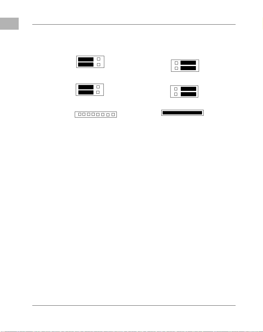
2 4 6
J10
1 3 5
2 4 6
J17
1 3 5
J4
1 2 3 4 5 6 7 8
PMC/SBC (761/IPMC) Mode Selection
There are five headers associated with the sele ction of the PMC or SBC
mode: J4, J6 J10, J17 and J20. Three of these headers are responsible for
secondary Ethernet I/O (J4, J10 and J17) to either the front panel (PMC
mode), or to the P2 connector via J4 (SBC mode). The other two headers
(J6 and J20) ensure proper routing of +/- 12V signal routing. The
MVME5100 is set at the fac tory for front pa nel I/O: PMC mode (see Ta ble
1-1). The SBC mode should only b e selected whe n using one of t he IPMC7xx modules in conjuncti on with the cor responding MVME7xx transiti on
module.
SBC I/O Mode
2 4 6
J10
1 3 5
2 4 6
J17
1 3 5
J4
1 2 3 4 5 6 7 8
For rear panel LAN, jumper
entire 8 pin header on J4
Installation Considerations
The MVME5100 draws power from th e VMEbus backplane connectors P1
and P2. Connector P2 is also used for the upper 16 bits of data in 32-bit
transfers, and for the upper 8 address lines in extended addressing mode.
The MVME5100 will not function properly without its main board
connected to VMEbus backplane connectors P1 and P2.
1-6 Computer Group Literature Center Web Site
Page 27

Preparation
Whether the MVME5100 operates as a VMEbus master or as a VMEbus
slave, it is configu red for 32 bit s of a ddress a nd 32 bi ts of data ( A32/D32).
However, it handles A16 or A24 devi ces in the appropriate a ddress ranges.
D8 and/or D16 devices in the system must be handled by the processor
software.
If the MVME5100 tries to access off-board resources in a nonexistent
location and if the system does not have a global bus time-out, the
MVME5100 waits indefinately for the VMEbus cycle to complete. This
will cause t he system to lock up. There is only one situation in which the
system might lack this global bus time-out; that is when the MVME5100
is not the system controller and there is no global bus time-out elsewhere
in the system.
Note Software can also disable the bus timer by settin g the appropriate
bits in the Universe II VMEbus interface.
Multiple MVME5100 boards may be installed in a single VME chassis;
however, each must have a unique VMEbus address. Other MPUs on the
VMEbus can interrupt, disable, communicate with, and determine the
operational status of the processor(s).
1
http://www.motorola.com/computer/literature 1-7
Page 28

Hardware Preparation and Installation
1
Installation
This section discusses the installation of PMCs onto the MVME5100,
installation of PMCspan modules onto the MVME5100, and the
installation of the MVME5100 into a VME chassis.
Note If you have ordered one or more of the optional RAM500
memory mezzanine boards for the MVME5100, ensure th at they
are installed on the board prior to proceeding. If they have not
been installed by the factory, and you are installing them
yourself, please refer to Appendix D, RAM500 Memory
Expansion Module, for installation instructions. It is
recommended that the memory mezz ainin e module s be i nstal led
prior to installing ot her board accessories, such as PMCs, IPMCs,
or transition modules.
1-8 Computer Group Literature Center Web Site
Page 29
Installation
0
1
J1
J22 J24 J12 J14
PCI MEZZANINE CARD
L1
J21 J23 J11 J13
L2
XU1 XU2
S1
PCI MEZZANINE CARD
HAWK
ASIC
U8
ABT/RST
BFL CPU
10/100 BASE T10/100 BASE T DEBUG
LAN 2 LAN 1
J15
J10 J17
J7
J16
J8
J25
P1 P2
J4
J3
J5
J6
J20
2788 0700
2788 070
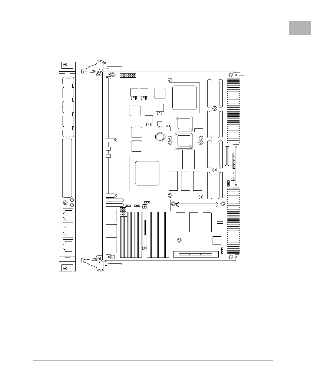
Figure 1-1. MVME5100 Layout
http://www.motorola.com/computer/literature 1-9
Page 30
Hardware Preparation and Installation
1
PMC Modules
PMC modules mount on top of the MVME5100. Perform the following
steps to install a PMC module on your MVME5100.
Dangerous voltages, capable of causing death, are present in this
equipment. Use extreme caution when handling, testing, and adjusting.
Warning
Inserting or removing modules with power applied may result in damage
to module components. Avoid touch ing areas of integr ated circuitry, st atic
Caution
discharge can damage these circuits.
Note This procedure assumes that you have read t he user’s manual that
came with your PMCs.
1. Attach an ESD strap to your wri st. Att ach the o ther en d of th e ESD
strap to an e lectrical ground. Note that the system chassis may not
be grounded if it is unplugged. The ESD strap must be secured to
your wrist and to ground throughout the procedure.
2. Perform an operating syst em shut down. Turn th e AC or DC power
off and remove the AC cord or DC power lines from the system.
Remove chassis or system cover(s) as necessary for access to the
VME modules.
3. If the MVME5100 has alread y been installed in a VMEb us card slot,
carefully remove it as shown in Figure 1-2 an d place it with
connectors P1and P2 facing you.
4. Remove the filler plate(s) from the front panel of the MVME5100.
5. Align the PMC module’s mating connectors to the MVME5100’s
mating connectors and press firmly into place.
6. Insert the appropriate number of Phillips screws (typically 4) from
the bottom of the MVME5100 into the standoffs on the PMC
module and tighten the screws (refer to Figure 1-3).
1-10 Computer Group Literature Center Web Site
Page 31

Installation
Figure 1-2. MVME5100 Installation and Removal From a VMEbus Chassis
1
Figure 1-3. Typical PMC Module Placement on an MVME5100
http://www.motorola.com/computer/literature 1-11
Page 32

Hardware Preparation and Installation
1
Primary PMCspan
To install a PMCspan-002 PCI expansion module on your MVME5100,
perform the following st ep s while referring to the figur e on th e next page:
Dangerous voltages, capable of causing death, are present in this
equipment. Use extreme caution when handling, testing, and adjusting.
Warning
Inserting or removing modules with power applied may result in damage
to module components. Avoid touch ing areas of integr ated circuitry, st atic
Caution
discharge can damage these circuits.
Note This procedure assumes that you have read t he user’s manual that
was furnished wit h your PMCspan and t hat you have instal led the
selected PMC modules on to your PMCspan according to the
instructions provided in the PMCspan and PMC manuals.
1. Attach an ESD strap to your wri st. Att ach the o ther en d of th e ESD
strap to an e lectrical ground. Note that the system chassis may not
be grounded if it is unplugged. The ESD strap must be secured to
your wrist and to ground throughout the procedure.
2. Perform an operating syst em shut down. Turn th e AC or DC power
off and remove the AC cord or DC power lines from the system.
Remove chassis or system cover(s) as necessary for access to the
VME modules.
3. If the MVME5100 has alread y been installed in a VMEb us card slot,
carefully remove it as shown in Figure 1-2 and place it with
connectors P1and P2 facing you.
4. Attach the four standoffs to the MVME5100. For each standoff:
– Insert the threaded end into the standoff hole at each corner of
the MVME5100.
– Thread the locking nuts into the standoff tips and tighten.
1-12 Computer Group Literature Center Web Site
Page 33

Installation
5. Place the PMCspan on top of the MVME5100. Al ign th e mounti ng
holes in each co rne r to the standoffs and align PMCspan connect or
P4 with MVME5100 connector J25.
PMCspan
MVME5100
1
2081 9708
Figure 1-4. PMCspan-002 Installation on an MVME5100
6. Gently press the PMCspan and MVME51 00 together and verify that
P4 is fully seated in J25.
http://www.motorola.com/computer/literature 1-13
Page 34

Hardware Preparation and Installation
1
7. Insert four short sc rews (Phillips type) through the holes at the
corners of the PMCspan and into the st andoffs on the MVME5100.
Tighten screws securel y.
Secondary
Warning
Caution
PMCspan
The PMCspan-010 PCI expansion module mounts on top of a
PMCspan-002 PCI expansion module. To insta ll a PMCspan-010 on your
MVME5100, perform the following steps whil e ref er ri ng t o the f igu re on
the next page:
Dangerous voltages, capable of causing death, are present in this
equipment. Use extreme caution when handling, testing, and adjusting.
Inserting or removing modules with power applied may result in damage
to module components. Avoid touch ing areas of integr ated circuitry, st atic
discharge can damage these circuits.
Note
T
his procedure assumes that you have read the user’s manual that
was furnished wit h the PMCsp an, and t hat you have inst alled t he
selected PMC modules on your PMCspan according to the
instructions provided in the PMCspan and PMC manual
1. Attach an ESD strap to your wri st. Att ach the o ther en d of th e ESD
strap to an e lectrical ground. Note that the system chassis may not
be grounded if it is unplugged. The ESD strap must be secured to
your wrist and to ground throughout the procedure.
s.
2. Perform an operating syst em shut down. Turn th e AC or DC power
off and remove the AC cord or DC power lines from the system.
Remove chassis or system cover(s) as necessary for access to the
VME module
3. If the Primary PMC Carrier Module and MVME5100 assembly is
already installed in the VME chassis, carefully remove it as shown
in Figure 1-2 and place it with connectors P1 and P2 facing you.
1-14 Computer Group Literature Center Web Site
Page 35

MVME5100 and
P
A
MCspan-002
ssembly
Installation
1
PMCspan-010
P3
J3
Figure 1-5. PMCspan-010 Installation on a PMCspan-002/MVME5100
4. Remove four screws (Phillips type) from the standoffs in each
corner of the primary PCI expansion module.
5. Attach the four standoffs from the PMCspan-010 mounting kit to
the PMCspan-002 by screwing the threaded male portion of the
standoffs in the locations where the screws were removed in the
previous step.
6. Place the PMCspan-010 on top of the PMCspan-002. Align the
mounting holes in each corner to the standoffs and align
PMCspan-010 connector P3 with PMCspan-002 connector J3.
http://www.motorola.com/computer/literature 1-15
Page 36

Hardware Preparation and Installation
1
7. Gently press the two PMCspan modules toget her and verify that P3
is fully sea ted in J3.
8. Insert the four screws (Phillips type) through the ho les at the corn ers
of PMCspan-010 and into the standoffs on the primary
PMCspan-002. Tighten screws securely.
Note The screws have two different head diameters. Use the screws
with the smaller heads on the standoffs next to VMEbus
connectors P1 and P2.
MVME5100
Before installing the MVME5100 in to you r VME ch ass is , ensure that the
jumpers are configured properly. This procedure assumes that you have
already installed the PMCspan(s) and any PMCs that you have selected.
Perform the following steps to install the MVME5100 in your VME
chassis:
Dangerous voltages, capable of causing death, are present in this
equipment. Use extreme caution when handling, testing, and adjusting.
Warning
Inserting or removing modules with power applied may result in damage
to module components. Avoid touch ing areas of integr ated circuitry, st atic
Caution
1-16 Computer Group Literature Center Web Site
discharge can damage these circuits
1. Attach an ESD strap to your wri st. Att ach the o ther en d of th e ESD
strap to an e lectrical ground. Note that the system chassis may not
be grounded if it is unplugged. The ESD strap must be secured to
your wrist and to ground throughout the procedure
2. Perform an operating syst em shut down. Turn th e AC or DC power
off and remove the AC cord or DC power lines from the system.
Remove chassis or system cover(s) as necessary for access to the
VME module
Page 37

Installation
3. Remove the filler pa nel from the VMEbus chassis card slot where
you are going to install the MVME5100. If you have installed one
or more PMCspan PCI expansio n modules onto your MVME5100,
you will need to remove filler panels from one additional card slot
for each PMCspan, above the card slot for the MVME5100.
– If you intend to use the MVME5100 as system c ontroller, it must
occupy the left-most card slot (slot 1) . The system controller
must be in slot 1 to correctly initiate the bus-grant daisy-chain
and to ensure proper operation of the IACK daisy-chain driver.
– If you do not int end to use the MVME5100 as system contro ller,
it can occupy any unused card slot.
4. Slide the MVME5100 (and PMCspans if used) into the selected
card slot(s). Ver ify t hat th e module o r module (s ) seat ed prop erly i n
the P1 and P2 connectors on th e chassi s backpl ane. Do not da mage
or bend connector pins.
5. Secure the MVME5100 (and PMCspans if us ed) in the chassis wi th
the screws in the top and bottom of its fr ont panel and verif y proper
contact with the transve rse mounting rails to minimize RF
emissions.
1
Note Some VME backplanes (such as those used in Motorola Modula r
Chassis systems) have an auto-jumpering featu re for automatic
propagation of the IACK and BG signals. The step immediately
below does not apply to such backplane designs.
6. On the chassis backplane, remove the
(IACK) and
BUS GRANT (BG) jumpers from the header for the card
INTERRUPT ACKNOWLEDGE
slots occupied by the MVME5100 and any PMCspan modules.
7. If you intend to use PPCbug interac tively, co nnect the terminal t hat
is to be used as the PPCbug system console to the
DEBUG port on
the front panel of the MVME5100.
Note In normal operation, the host CPU controls MVME5100
operation via the VMEbus Universe registers.
http://www.motorola.com/computer/literature 1-17
Page 38

Hardware Preparation and Installation
1
8. Replace the chassis or system cover(s) and cable peripherals to the
panel connectors as required.
9. Reconnect the system to the AC or DC power source and turn the
system power on.
10. The MVME5100’s green
CPU LED indicates activity as a set of
confidence tests is run, and the debugger prompt
appears.
PPC6-Bug>
1-18 Computer Group Literature Center Web Site
Page 39

Introduction
This chapter provides operating instructions for the MVME5100 Single
Board Computer. It includes neces sary information abo ut powering up the
system along with the functionality of the switches, status indicators, and
I/O ports on the front panels of the board.
Switches and Indicators
The front panel of the MVME5100 as shown in Figure 1-1, incorporates
one dual function tog gle swit ch
(LED) status indicator s (
ABT/RST Switch
BFL, CPU) located on the front pa nel.
2Operation
2
(ABT/RST) and two Light-Emitting Di ode
Abort Function
Reset Function
The ABT/RST switch operates in the following manner: if pressed for less
than 5 seconds, t he
seconds, the
When toggled to
processor. The interrupt is normally used to abort program execution and
return control to the debugger firmware located in the processor and flash
memory.
The interrupt signal rea ches the processor via ISA bus interrupt line IRQ8.
The interrupter c onnected to th e
filtered to remove switch bounce.
When toggled to
reset, the switch must be depressed for more than five seconds.
ABORT function is selected, if presse d for more tha n 5
RESET function is sele cted. Eac h functi on is de scribed below.
ABT, the switch generates an interrupt signal to the
ABORT switch is an edge-sensitive circuit,
RST, the switch resets all onboar d devices. To ge nerate a
2-1
Page 40

Operation
2
The on-board Universe ASIC includes both a global and a local reset
driver. When the ASIC operates as the System Controller, the reset driver
provides a global system reset by asserting the SYSRESET# signal.
Additionaly, when the MVME5100 is configured as a System Controller
(SCON), a SYSRESET# signal may be gen erated by toggling the
switch to RST, or by a power-up reset, or by a watchdog timeout, or by a
control bit in the Miscellan eous Control Register (MISC_ CTL) in the
Universe ASIC.
Note SYSRESET# remains asserted for at least 200 ms, as
Status Indicators
There are two Light-E mitting Diode (LED) stat us indicators locate d on the
MVME5100 front panel. They are labeled
RST Indicator (DS1)
ABT/RST
required by the VMEbus specification.
BFL and CPU.
The yellow
illuminated during reset as an LED test. The
BFL LED indicates board failure; this indicator is also
BFL is set if the MODFAIL
Register o r FUSE Regist er is set. Refer to the MVME5100 Single Board
Computer Programmer’s Reference Guide (V5100A/PG) for information
on these registers.
CPU Indicator (DS2)
The green
CPU LED indicates CPU activity.
Connectors
There are three conn ectors on the fro nt panel o f the MVME510 0. Two are
bottom-labeled
2-2 Computer Group Literature Center Web Site
10/100BASE T and one is labeled DEBUG.
Page 41

System Powerup
10/100 BASE T Ports
The two RJ-45 ports labeled
10BaseT/100BaseTX Ethernet LAN interface. These connectors are toplabeled with the designation
DEBUG Port
The RJ-45 port labeled
interface, based on TL16C550 Universal Asynchronous
Receiver/Transmitter (UART) controller chip. It is asynchronous only.
For additional information on pin assignments, refer to Cha pt er 5, Pin
Assignments.
The
DEBUG port may be used for conne cting a terminal to the MVME5 100
to serve as t he firmware console for the factory inst alled debugger,
PPCBug. The port is configured as follows:
❏ 8 bits per character
❏ 1 stop bit per character
❏ Parity disabled (no parity)
❏ Baud rate = 9600 baud (default baud rate at power-up)
2
10/100 BASE T provide the
LAN1 and LAN2.
DEBUG provides an RS232 serial communi cations
After power-up, the baud rate of the
DEBUG port can be reconfigured by
using the debugger’s Port Format (PF) command.
System Powerup
After you have verified that all necessary hardware preparation is done,
that all connections were made correctly, and that the installation is
complete, you can power up the system.
http://www.motorola.com/computer/literature 2-3
Page 42

Operation
2
Initialization Process
The MPU, hardware, and firmware initialization process is performed by
the PPCBug firmware upon s ystem powerup or system res et. The firmware
initializes the devices on the MVME5100 in preparation for booting an
operating system.
The firmware is shipped from the factory with an appropriate set of
defaults. Dependin g on your system a nd specific application , there may or
may not be a need to modify the firmware configuration before you boot
the operating system. If it is necessary, refer to Chapter 3 , PPCBug
Firmware for addition al information on modifying firmware defa ult
parameters.
The following flowchart in Figure 2-1 shows the basic initialization
process that takes place during MVME5100 system start-ups.
For further information on PPCBug, refer to the following:
❏ Chapter 3, PPCBug Firmware
❏ Appendix B, Troubleshooting
❏ Appendix C, Related Documentat ion
2-4 Computer Group Literature Center Web Site
Page 43

System Powerup
2
STAR TUP
INITIALIZATION
POST
BOOTING
MONITOR
Powerup/reset initialization
Initialize devices on the MVME5100
PowerOn Self-Test diagnostics
Firmware-configured boot mech ani sm
if so configured. Default is no boot.
,
Interactive, command-driven on-line PPC
debugger, when terminal connected.
Figure 2-1. Boot-Up Sequence
http://www.motorola.com/computer/literature 2-5
Page 44

Page 45

3PPCBug Firmware
Introduction
The PPCBug firmware is the layer of software just a bove the hardware.
The firmware provides the proper initialization for the devices on the
MVME5100 upon powerup or reset.
This chapter describes the basics of the PPCBug and its a rchitecture. It also
describes the monitor (interactiv e command portion of th e firmware), and
provides information on using the PPCBug debugger and the special
commands. A complete list of PPCBug commands is also provided.
For full user information about PPCBug, refer to the PPCBug Firmware
Package User’s Manual and the PPCBug Diagnostics Manual, listed in
Appendix C, Related Documentat ion.
PPCBug Overview
3
The PPCBug debugger firmware is a powerful evaluation and debugging
tool for systems built around Motorola microprocessor. Facilities are
available for loading and executing user programs under complete
operator control for system evaluation. The PPCBug provides a high
degree of functionality, user friendliness, portability, and ease of
maintenance.
The PPCBug also achieves its portability because it was written entirely in
the C programming language, except where necessary to use assembler
functions.
PPCBug includes com mands for:
❏ Display and modification of memory
❏ Breakpoint and tracing capabilities
❏ A powerful assembler and disassembler useful for patching
programs
3-1
Page 46

PPCBug Firmware
3
❏ A self-test at powerup feature which verifies the integrity of the
system
PPCBug consists of three parts:
❏ A command-driven, user-interactive software debugger, described
in the PPCBug Firmware Package User’s Manual, listed in
Appendix C, Related Documentat ion (hereafter referred to as
“debugger” or “PPCBug”).
❏ A command-driven diagnostics package for the MVME5100
hardware (hereafter referred to as “diagnostics”). The diagnostics
package is described in the PPCBug Diagnostics Manual, listed in
Appendix C, Related Documentat ion.
❏ A user interface or debug/diagnostics monitor that accepts
commands from the system console terminal.
When using PPCBug, you operate out of e ither the debugger directory or
the diagnostic directory.
❏ If you are in the debugger directory, the debugger prompt
PPC6-Bug> is displayed and you have all of the debugger
commands at your disposal.
❏ If you are in the diagnostic directory, the diagnostic prompt
PPC6-Diag>
is displayed and you have all of the diagnostic
commands at your disposal as well as all of the debugger
commands.
Because PPCBug is command-driv en, it performs it s various operat ions in
response to user commands entered at the keyboard. When you enter a
command, PPCBug executes the command and the prompt reappears.
However, if you enter a command that causes executi on of user target co de
(for example, GO), then control may or may not return to PPC Bug,
depending on the outcome of the user program.
3-2 Computer Group Literature Center Web Site
Page 47

Implementation and Memory Requirements
PPCBug is written largely in the C programming language, providing
benefits of portability and maintai nability. Where necessa ry, assembly
language has been used in the form of separately compiled program
modules containing only assembler code.
Physically, PPCBug is contained in two socketed 32-pin PLCC Flash
devices that together provide 1MB of storage. The executable code is
checksummed at every power-on or reset firmware entry. The result
(which includes a pr ecalcula ted checks um contained in the flash de vices),
is verified against the expected checksum.
PPCBug requires a maximum of 768KB of read/write memory. The
debugger allocates this space from the top of memory. For example, a
system containing 64MB (0x04000000) of read/write memory will place
the PPCBug memory locations 0 x03F40000 to 0 x3FFFFFF. Additionall y,
the first 1MB of DRAM is reserved for the exception vector table and
stack.
Using PPCBug
3
Using PPCBug
PPCBug is command-driven; it pe rforms its various operatio ns in response
to commands that you enter a t the k eyboard. Whe n the
appears on the screen, the debugger is ready to accept debugger
commands. When the
debugger is ready to accept diagnostics commands. To switch from one
mode to the other, enter SD.
What you enter is store d i n an int ernal buff er. Exec ution b egins o nly afte r
you press the Return or Enter key. This allows you t o correct entry error s,
if necessary, with the control characters described in the PPCBug
Firmware Package User’s Manual, listed in Appendix C, Related
Documentation.
After the debugger executes the command, the prompt reappears.
However, depending on what the user program does, if the command
causes execution of a user target code (that is, GO), then control may or
may not return to the debugger.
http://www.motorola.com/computer/literature 3-3
PPC6-Diag> prompt appears on the screen, the
PPC6-Bug> prompt
Page 48

PPCBug Firmware
3
For example, if a bre akpoint has bee n specified, t hen control re turns to the
debugger when the breakpoint is enc ountered during e xecution of the user
program. Alternately, the user program could return to the debugger by
means of the System Call Handler routine RETURN (described in the
PPCBug Firmware Package User’s Manu al). For more about this, refer to
the GD, GO, and GT command descriptions in the PPCBug Firmware
Package User’s Manual, listed in Appendix C, Related Documentation .
A debugger command is made up of the following parts:
❏ The command name, either uppercase or lowercase (for example,
MD or md)
❏ Any required arguments, as specified by command
❏ At least one s pace before the first argume nt. Precede all other
arguments with either a space or comma.
❏ One or more options. Precede an option or a string of options with
a semicolon (;). If no option is entered, the command’s default
option conditions are used.
Hardware and Firmware Initialization
The debugger performs the hardware and firmware initialization process.
This process occurs each time the MVME5100 is reset or powered up. The
steps listed below are a high-level outline; be aware that not all of the
detailed steps are listed.
1. Sets MPU.MSR to known value.
2. Invalidates the MPU's data/instruction caches.
3. Clears all segment registers of the MPU.
4. Clears all block address translation registers of the MPU.
5. Initializes the MPU-bus-to-PCI-bus bridge device.
6. Initializes the PCI-bus-to-ISA-bus bridge device.
7. Calculates the external bus clock speed of the MPU.
3-4 Computer Group Literature Center Web Site
Page 49

8. Delays for 750 milliseconds.
9. Determines the CPU base board type.
Using PPCBug
10. Sizes th e local read/write memory (that is, DRAM).
11. Initializes the read/write memo ry controller. Sets base add ress of
memory to 0x00000000.
12. Retrieves the speed of read/write memory.
13. Initializes the read/write memory controller with the speed of
read/write m emory.
14. Retrieves the speed of read only memory (that is, Flash).
15. Initializes the read only memory controller with the speed of read
only memory.
16. Enables the MPU's instruction cache.
17. Copies the MPU's exception vector table from 0xFFF00000 to
0x00000000.
18. Verifies MPU type.
19. Enables the superscalar feature of the MPU (superscalar processor
boards only).
20. Verifies the external bus clock speed of the MPU.
3
21. Determines the debugger's console/host ports and initializes the
PC16550A.
22. Displays the debugger's copyright message.
23. Displays any hardware initial i zat ion errors that may have occurred.
24. Checksums the debugger obj ect and disp la ys a warning message if
the checksum failed to verify.
25. Displays the amount of local read/write memory found.
26. Verifies the configuration data that is resident in NVRAM and
displays a warning message if the verification failed.
http://www.motorola.com/computer/literature 3-5
Page 50

PPCBug Firmware
3
27. Calculates and displ ays the MPU clock spee d, verifies that the MPU
clock speed matches the configura tion data , and displ ays a warni ng
message if the verification fails.
28. Displays the BUS clock speed, verifies that the BUS clock speed
matches the configuration data, and displays a warning message if
the verific ation fails.
29. Probes PCI bus for supported network devices.
30. Probes PCI bus for supported mass storage devices.
31. Initializes the memory/IO addresses for the supported PCI bus
devices.
32. Executes Self-Test, if so configured. (Default is no Self-Test).
33. Extinguishes the board fail LED, if Self-Test passed, and outputs
any warning messages.
34. Executes boot program, if so configured. (Default is no boot.)
35. Executes the debugger monitor (that is, issues the
prompt).
PPC6-Bug>
Default Settings
The following sections provide information pertaining to the firmware
settings of the MVME5100. Default (factory set) Environment (ENV)
commands are provided to inform you on how the MVME5100 was
configured at the time it left the factory.
3-6 Computer Group Literature Center Web Site
Page 51

CNFG - Configure Board Information Block
Use this command to disp lay and config ure the Board I nformat ion Block,
which is resident within the NVRAM. This data block contains various
elements detailing specific operational parameters of the MVME5100.
The structure for the board is shown in the following example:
Board (PWA) Serial Number = MOT00xxxxxxx
Board Identifier = MVME5100
Artwork (PWA) Identifier = 01-W3518FxxB
MPU Clock Speed = 450
Bus Clock Speed = 100
Ethernet Address = 0001AF2A0A57
Primary SCSI Identifier = 07
System Serial Number = nnnnnnnn
System Identifier = Motorola MVME5100
License Identifier = nnnnnnnn
Default Settings
3
The Board Information Block parameters shown above are left-justified
character (ASCII) strings padded with space characters.
The Board Information Block is factory-configured before shipment.
There is no need to modify block parameters unless the NVRAM is
corrupted.
Refer to the PPCBug Firmware Package User's Manual, listed in
Appendix C, Related Documentat ion for a description of CNFG and
examples.
ENV - Set Environment
Use the ENV command to vi ew and/or confi gure interactiv ely all PPCBug
operational parameters that are kept in Non-Volatile RAM (NVRAM).
http://www.motorola.com/computer/literature 3-7
Page 52

PPCBug Firmware
3
Refer to the PPCBug Firmware Package User's Manual for a des cr ipt io n
of the use of ENV. Additional in formation on registers in the Universe
ASIC that affect these parameters is contained in your MVME5100
Programmer’s Reference Guide, listed in Appendix C, Related
Documentation.
Listed and described below are the parameters that you can configure
using ENV. The default values shown were those in effect when this
publication went to print.
Configuring the PPCBug Parameters
The parameters that can be configured using ENV are:
Bug or System environment [B/S] = B?
B Bug is the mode where no system type of support is
displayed. However, system-related items are still
available. (Default)
S System is the standard mode of operation, and is the
default mode if NVRAM should fail . S ys tem mode i s
defined in the PPCBug Firmware Package User's
Manual listed in Appendix C, Related
Documentation.
Maximum Memory Usage (MB,0=AUTO) = 1?
This parameter specifies the maximum number of megabytes the bug is
allowed to use. Allocation begins at the top of physical memory and
expands downward as more memory i s req uired until th e maximum va lue
is reached.
If a value of zero is specif ied, memory will continue to be increas ed as
needed until half of the available memory is consumed (that is, 32MB in a
64MB system). This mode is useful for determining the full memory
required for a specific conf iguration. Once this is determ ined, a hard value
may be given to th e paramete r and it is guar anteed t hat no memor y will be
used over this amount.
The default value for this parameter is one.
3-8 Computer Group Literature Center Web Site
Page 53

Default Settings
Note: The bug does not automatically acquire all of the memory it is
allowed. It accumulates memory as necessary in one megabyte
blocks.
Field Service Menu Enable [Y/N] = N?
Y Display the field service menu.
N Do not display the field service menu. (Default)
Remote Start Method Switch [G/M/B/N] = B?
The Remote Start Method Switch is used when the MVME5100 is crossloaded from another VME-based CPU in order to start execution of the
cross-loaded program.
G Use the Global Control and Status Register to pass
and start execution of the cross-loaded program.
M Use the Multiprocessor Control Register (MPCR) in
shared RAM to pass and start execution of the crossloaded program.
3
B Use both the GCSR and the MPCR methods to pass
and start execution of the cross-loaded program.
(Default)
N Do not use any Remote Start Method.
Probe System for Supported I/O Controllers [Y/N] = Y?
Y Accesses will be made to the appropriate system
buses (for example, VMEbus, local MPU bus) to
determine the presence of supported controllers.
(Default)
N Accesses will not be made to the VMEbus to
determine the presence of supported controllers.
http://www.motorola.com/computer/literature 3-9
Page 54

PPCBug Firmware
3
Auto-Initialize of NVRAM Header Enable [Y/N] = Y?
Y NVRAM (PReP partition) header space will be
initialized automatically during board initialization,
but only if the PReP partition fails a sanity check.
(Default)
N NVRAM header space will not b e init ialized
automatically during board initialization.
Network PReP-Boot Mode Enable [Y/N] = N?
Y Enable PReP-style network booting (same boot image
from a network interface as from a mass storage
device).
N Do not enable PReP- sty le network booting. (Default)
Negate VMEbus SYSFAIL* Always [Y/N] = N?
Y Negate the VMEbus SYSFAIL
∗ signal during board
initialization.
N Negate the VMEbus SYSFAIL
∗ signal after
successful completion or entrance into the bug
command monitor. (Default)
SCSI Bus Reset on Debugger Startup [Y/N] = N?
Y Local SCSI bus is reset on debugger setup.
N Local SCSI bus is not reset on debugger setup.
(Default)
Primary SCSI Bus Negotiations Type [A/S/N] = A?
A Asynchronous SCSI bus negotiation. (Default)
S Synchronous SCSI bus negotiation.
N None.
3-10 Computer Group Literature Center Web Site
Page 55

Primary SCSI Data Bus Width [W/N] = N?
W Wide SCSI (16-bit bus).
Default Settings
N Narrow SCSI (8-bit bus). (Default)
Secondary SCSI identifier = 07?
Select the identifier. (Default = 07.)
NVRAM Bootlist (GEV.fw-boot-path) Boot Enable [Y/N] = N?
Y Give boot priority to devices defined in the fw-boot-
path global environment variab le (GEV).
N Do not give boot prior ity to devices listed in the fw-
boot-path GEV. (Default)
Note When enabled, the GEV boot takes priority over all other boots,
including Autoboot and Network Boot.
NVRAM Bootlist (GEV.fw-boot-path) Boot at power-up only [Y/N] = N?
Y Give boot priority to devices defined in the fw-boot-
path GEV at powerup reset only.
N Give powerup boot priority to devices listed in the fw-
boot-path GEV at any reset. (Default)
3
NVRAM Bootlist (GEV.fw-boot-path) Boot Abort Delay = 5?
The time (in seconds) that a boot from the NVRAM boot list will delay
before starting the boot. The purpose for the delay is to allow you the
option of stopping the boot by use of the
BREAK key. The time value is
from 0-255 seconds. (Default = 5 seconds)
Auto Boot Enable [Y/N] = N?
Y The Autoboot functio n is enabled .
N The Autoboot functio n is disabled. (Default)
http://www.motorola.com/computer/literature 3-11
Page 56

PPCBug Firmware
3
Auto Boot at powerup only [Y/N] = N?
Y Autoboot is attempted at powerup reset only.
N Autoboot is attempted at any reset. (Default)
Auto Boot Scan Enable [Y/N] = Y?
Y If Autoboot is enabled, the Autoboot process attempts
to boot from devices specified in the scan list (for
example,
N If Autoboot is enabled, the Autoboot process uses the
Controller LUN and Device LUN to boot.
Auto Boot Scan Device Type List = FDISK/CDROM/TAPE/HDISK?
FDISK/CDROM/TAPE/HDISK). (Default)
This is the listing of boot devices di splayed if the Autoboot Sca n option is
enabled. If you modify the list , follow the format sho wn above (uppercase
letters, us ing forward s lash as separator).
Auto Boot Controller LUN = 00?
Refer to the PPCBug Firmware Package User's Manual for a listing of
disk/tape controller modules currently supported by PPCBug. (Default =
0x00)
Auto Boot Device LUN = 00?
Refer to the PPCBug Firmware Package User's Manual listed in
Appendix C, Related Documentat ion for a listing of disk/tape devices
currently supported by PPCBug. (Default = 0x00)
Auto Boot Partition Number = 00?
Identifies which disk “partition” is to be booted, as specified in the
PowerPC Reference Platform (PReP) specification. If set to zero, the
firmware will search the partitions in order (1, 2, 3, 4) until it finds the first
“bootable” partition. That is then the partition that will be booted. Other
acceptable values are 1, 2, 3, or 4. In these four cases, the partition
specified will be booted without searching.
3-12 Computer Group Literature Center Web Site
Page 57

Default Settings
Auto Boot Abort Delay = 7?
The time in seconds that the Autoboot sequence w i ll delay befo re
starting the boot. The pu rpose for the delay is to a ll ow you t he option
of stopping the boo t by use of the
BREAK key. The time value is from
0-255 seconds. (Default = 7 seconds)
Auto Boot Default String [NULL for an empty string] = ?
You may specify a string (filename) which is passed on to the code
being booted. The maximum length of this string is 16 characters.
(Default = null string)
ROM Boot Enable [Y/N] = N?
Y The ROMboot function is enabled .
N The ROMboot function is disabl ed. (Default)
ROM Boot at power-up only [Y/N] = Y?
Y ROMboot is attempted at power-up only. (Default)
N RO Mboo t is attempted at any reset.
3
ROM Boot Enable search of VMEbus [Y/N] = N?
Y VMEbus address sp ace, in add ition to the usual areas
of memory, will be searched for a ROMboot module.
N VMEbus address space will not be accessed by
ROMboot. (Default)
ROM Boot Abort Delay = 5?
The time (in seconds) that the ROMboot sequence will delay before
starting the boot. The purpose for the delay is to allow you the option of
stopping the boot by u se o f t h e
BREAK key. The time value is fr om 0-255
seconds. (Default = 5 seconds)
ROM Boot Direct Starting Address = FFF00000?
The first location tested when PPCBug searches for a ROMboot module.
(Default = 0xFFF00000)
http://www.motorola.com/computer/literature 3-13
Page 58

PPCBug Firmware
3
ROM Boot Direct Ending Address = FFFFFFFC?
The last location tested when PPCBug searches for a ROMboot module.
(Default = 0xFFFFFFFC)
Network Auto Boot Enable [Y/N] = N?
Y The Network Auto Boot (NETboot) function is
enabled.
N The NETboot function is disabled. (Default)
Network Auto Boot at power-up only [Y/N] = N?
Y NETboot is attempted at powerup reset only.
N NETboot is attempted at any reset. (Default)
Network Auto Boot Controller LUN = 00?
Refer to the PPCBug Firmware Package User's Manual, listed in
Appendix C, Related Documentat ion for a listing of network controller
modules currently supported by PPCBug. (Default = 0x00)
Network Auto Boot Device LUN = 00?
Refer to the PPCBug Firmware Package User's Manual, listed in
Appendix C, Related Documentat ion for a listing of network controller
modules currently supported by PPCBug. (Default = 0x00)
Network Auto Boot Abort Delay = 5?
The time in seconds that the NETboot sequence will delay before starting
the boot. The purpose for the delay is to allow you the option of stopping
the boot by use of the
BREAK key. The time value is from 0-255 secon ds.
(Default = 5 seconds)
Network Auto Boot Configuration Parameters Offset (NVRAM) =
00001000?
The address where the network interface configuration parameters are to
be saved/retained in NVRAM; these parameters are the necessary
parameters to perf orm an unattende d network boot . A typical offset migh t
be 0x1000, but this value is application-specific. (Default = 0x00001000)
3-14 Computer Group Literature Center Web Site
Page 59

!
Caution
Default Settings
If you use the NIOT debugger command, these parameters need to be
saved somewhere in the offset range 0x00001000 through 0x000016F7.
The NIOT parameters do not exceed 12 8 bytes i n size. The setti ng of thi s
ENV pointer determines their l ocation. If you have used the sa me space for
your own program informat ion or commands, they will be ove rwritten and
lost.
You can relocate the network interface configuration paramet ers in this
space by using the ENV command to change the Network Auto Boot
Configuration Parameters Offset from its default of 0x00001000 to the
value you need to be clear of your data within NVRAM.
Memory Size Enable [Y/N] = Y?
Y Memory will b e sized for SelfTest diagnostics.
(Default)
N Memory will not be sized for SelfTest diagnostics.
3
Memory Size Starting Address = 00000000?
The default Starting Address is 0x00000000.
Memory Size Ending Address = 02000000?
The default Ending Address is the calculated size of local memory. If the
memory start is changed from 0x0x0 00000 00, this value wil l also nee d to
be adjusted.
DRAM Speed in NANO Seconds = 15?
The default set ti ng fo r this parameter will vary dependin g on t h e spe ed of
the DRAM memory parts installed on the board. The defaul t is set to the
slowest speed found on the available banks of DRAM memory.
ROM Bank A Access Speed (ns) = 80?
This defines the minimum access speed for the Bank A Flash Device(s) in
nanoseconds.
http://www.motorola.com/computer/literature 3-15
Page 60

PPCBug Firmware
3
ROM Bank B Access Speed (ns) = 70?
This defines the minimum access speed for the Bank B Flash
Device(s) in nanoseconds.
DRAM Parity Enable [On-Detection/Always/Never - O/A/N] = O?
O DRAM parity is enabled upon detection. (Default)
A DRAM parity is always enabled.
N DRAM parity is never enabled.
Note This parameter also applies to enabling ECC for DRAM.
L2 Cache Parity Enable [On-Detection/Always/Never - O/A/N] = O?
O L2 Cache parity is enabled upon detection. (Default)
A L2 Cache parity is always enabled.
N L2 Cache parity is never enabled.
PCI Interrupts Route Control Registers (PIRQ0/1/2/3) = 0A0B0E0F?
Initializes the PIRQx (PCI Interrupts) route control registers in the IBC
(PCI/ISA bus bridge controller). The ENV parameter is a 32-bit v alue that
is divided by 4 fields to specify the values for route control registers
PIRQ0/1/2/3. The default is determined by system type as shown:
PIRQ0=0A, PIRQ1=0B, PIRQ2=0E, PIRQ3=0F.
LED/Serial Startup Diagnostic Codes
These codes can be displayed at key points in the initialization of the
hardware devices. The codes are enabled by an ENV parameter.
Serial Startup Code Master Enable [Y/N]=N?
Should the debugger fail to come up to a prompt, the last code displayed
will indicate how far the initialization sequence had progressed before
stalling.
3-16 Computer Group Literature Center Web Site
Page 61

Serial Startup Code LF Enable [Y/N]=N?
Default Settings
A line feed c an be inserted after each code is displayed to prevent it from
being overwritten by the next code. This is also enabled by an ENV
parameter:
The list of LED/serial codes is in cluded in the section on MPU, Hardware ,
and Firmware Initialization found in Chapter 1 of th e PPCBug Fi rmware
Package User’s Manual, listed in Appendix C, Related Documentation.
Configuring the VMEbus Interface
ENV asks the following serie s of questions to set up the VMEbus interface
for the MVME5100. To perform this configuration, you should have a
working knowledge of the Universe ASIC as described in your
MVME5100 Programmer’s Reference Guide. Also, refe r to the Tundra
Universe II Users Manual, as listed in Appendix C, Related
Documentation for a detailed description of VMEbus addressing. In
general, the PCI slave images describe the VME master addresses, while
the VMEbus slave describes the VME slave addres ses.
VME3PCI Master Master Enable [Y/N] = Y?
Y Set up and enable the VMEbus Interface. (Default)
N Do not set up or enable the VMEbus Interface.
3
PCI Slave Image 0 Control = 00000000?
The configured value is written into the LSI0_CTL re gister of the Universe
chip.
PCI Slave Image 0 Base Address Register = 00000000?
The configured value is wr itte n into t he LSI0_BS re gist er of th e Univ erse
chip.
PCI Slave Image 0 Bound Address Register = 00000000?
The configured value i s writte n into the LSI0_BD regi ster of t he Univers e
chip.
PCI Slave Image 0 Translation Offset = 00000000?
http://www.motorola.com/computer/literature 3-17
Page 62

PPCBug Firmware
3
The configured value is written into t he LSI0_TO reg ister of the Uni verse
chip.
PCI Slave Image 1 Control = C0820000?
The configured value is written into the LSI1_CTL re gister of the Universe
chip.
PCI Slave Image 1 Base Address Register = 81000000?
The configured value is wr itte n into t he LSI1_BS re gist er of th e Univ erse
chip.
PCI Slave Image 1 Bound Address Register = A0000000?
The configured value i s writte n into the LSI1_BD regi ster of t he Univers e
chip.
PCI Slave Image 1 Translation Offset = 80000000?
The configured value is written into t he LSI1_TO reg ister of the Uni verse
chip.
PCI Slave Image 2 Control = C0410000?
The configured value is written into the LSI2_CTL re gister of the Universe
chip.
PCI Slave Image 2 Base Address Register = A0000000?
The configured value is wr itte n into t he LSI2_BS re gist er of th e Univ erse
chip.
PCI Slave Image 2 Bound Address Register = A2000000?
The configured value i s writte n into the LSI2_BD regi ster of t he Univers e
chip.
PCI Slave Image 2 Translation Offset = 500000000?
The configured value is written into t he LSI2_TO reg ister of the Uni verse
chip.
PCI Slave Image 3 Control = C0400000?
The configured value is written into the LSI3_CTL re gister of the Universe
chip.
PCI Slave Image 3 Base Address Register = AFFF0000?
3-18 Computer Group Literature Center Web Site
Page 63

Default Settings
The configured value is wr itte n into t he LSI3_BS re gist er of th e Univ erse
chip.
PCI Slave Image 3 Bound Address Register = B0000000?
The configured value i s writte n into the LSI3_BD regi ster of t he Univers e
chip.
PCI Slave Image 3 Translation Offset = 50000000?
The configured value is written into t he LSI3_TO reg ister of the Uni verse
chip.
VMEbus Slave Image 0 Control = E0F20000?
The configured value is written into the VSI0_CTL register of the
Universe chip.
VMEbus Slave Image 0 Base Address Register = 00000000?
The configured value is written into the VSI0_BS register of the Universe
chip.
VMEbus Slave Image 0 Bound Address Register = (Local DRAM Size)?
3
The configured value is written int o the VSI0_BD regis ter of the Univers e
chip. The value is the same as the Local Memory Found number already
displayed.
VMEbus Slave Image 0 Translation Offset = 00000000?
The configured value is written into the VSI0_TO register of the Universe
chip.
VMEbus Slave Image 1 Control = 00000000?
The configured value is written into the VSI1_CTL register of the
Universe chip.
VMEbus Slave Image 1 Base Address Register = 00000000?
The configured value is written into the VSI1_BS register of the Universe
chip.
VMEbus Slave Image 1 Bound Address Register = 00000000?
The configured value is written int o the VSI1_BD regis ter of the Univers e
chip.
http://www.motorola.com/computer/literature 3-19
Page 64

PPCBug Firmware
3
VMEbus Slave Image 1 Translation Offset = 00000000?
The configured value is written into the VSI1_TO register of the Universe
chip.
VMEbus Slave Image 2 Control = 00000000?
The configured value is written into the VSI2_CTL register of the
Universe chip.
VMEbus Slave Image 2 Base Address Register = 00000000?
The configured value is written into the VSI2_BS register of the Universe
chip.
VMEbus Slave Image 2 Bound Address Register = 00000000?
The configured value is written int o the VSI2_BD regis ter of the Univers e
chip.
VMEbus Slave Image 2 Translation Offset = 00000000?
The configured value is written into the VSI2_TO register of the Universe
chip.
VMEbus Slave Image 3 Control = 00000000?
The configured value is written into the VSI3_CTL register of the
Universe chip.
VMEbus Slave Image 3 Base Address Register = 00000000?
The configured value is written into the VSI3_BS register of the Universe
chip.
VMEbus Slave Image 3 Bound Address Register = 00000000?
The configured value is written int o the VSI3_BD regis ter of the Univers e
chip.
VMEbus Slave Image 3 Translation Offset = 00000000?
The configured value is written into the VSI3_TO register of the Universe
chip.
PCI Miscellaneous Register = 10000000?
The configured value is written into the LMISC register of the Universe
chip.
3-20 Computer Group Literature Center Web Site
Page 65

Default Settings
Special PCI Slave Image Register = 00000000?
The configured value is written into the SLSI registe r of the Universe chip.
Master Control Register = 80C00000?
The configured value is written into the MAST_CTL register of the
Universe chip.
Miscellaneous Control Register = 52060000?
The configured value is written into the MISC_CTL register of the
Universe chip.
User AM Codes = 00000000?
The configured value is written into the USER_AM register of the
Universe chip.
Firmware Command Buffer
Firmware Command Buffer Enable = N?
Y Enables Firmware Command Buffer execution.
N Disables Firmware Command Buffer execution
(Default).
Firmware Command Buffer Delay = 5?
Defines the number of seconds to wait before firmware begins executing
the startup commands in the startup command buffer. During this delay,
you may press any key to prevent the execution of the startup command
buffer.
3
The default value of this parameter causes a startup delay of 5 seconds.
Firmware Command Buffer:
['NULL' terminates entry]?
The Firmware Command Buffer contents contain the BUG commands
which are executed upon firmware startup.
BUG commands you place into the command buffer shoul d be typed just
as you enter the commands from the command line.
http://www.motorola.com/computer/literature 3-21
Page 66

PPCBug Firmware
3
The string 'NULL' on a new line terminates the command line entries.
All PPCBug commands, except for the followin g, may be us ed within
the command buffer: DU, ECHO, LO, TA, VE.
Note Interactive editing of the startup command buffer is not
supported. If changes are needed to an existing set of startup
commands, a new set of commands with changes must be
reentered.
Standard Commands
The individual debugger commands are listed in the following table. The
commands are described in detail in the PPCBug Firmware Package
User’s Manual, listed in Appendix C, Related Documentation.
Note You can list all the availabl e debugger commands by enterin g the
Help (HE) command alone. You can view the syntax for a
particular command by entering HE and the command
mnemonic, as listed below.
Table 3-1. Debugger Commands
Command Description
AS Assembler
BC Block of Memory Compare
BF Block of Memory Fill
BI Block of Memory Initialize
BM Block of Memory Move
BS Block of Memory Search
BR Breakpoi n t Ins ert
BV Block of Memory Verify
CACHE Modify Cache State
CM Concurrent Mode
3-22 Computer Group Literature Center Web Site
Page 67

Standard Commands
Table 3-1. Debugger Commands (Continued)
Command Description
CNFG Configure Board Information Block
CS Checksum a Block of data
CSAR PCI Configuration Space READ Access
CSAW PCI Configuration Space WRITE Access
DC Data Conversion and Expression Evaluation
DE Detect Errors
DS Disassembler
DU Dump S-Records
ECHO Echo St ring
ENV Set Environment to Bug/Operating System
FORK Fork Idle MPU at Address
FORKWR Fork Idle MPU with Registers
G “Alias” for “GO” Command
GD Go Direct (Ignore Breakpoints)
GEVBOOT Global En vironment Variable Boot - Bootstrap Operating
System
GEVDEL Global Environment Variable Delete
GEVDUMP Global Environment Variable(s) Dump (NVRAM Header +
Data)
GEVEDIT Global Environment Variable Edit
GEVINIT Global Environment Variable Initialize (NVRAM Header)
GEVSHOW Global Environment Variable Show
GN Go to Next Instruction
GO Go Execute User Program
GT Go to Temporary Breakpoint
HE Help on Command(s)
IBM Indirect Block Move
IDLE Idle Master MPU
IOC I/O Control for Disk
3
http://www.motorola.com/computer/literature 3-23
Page 68

PPCBug Firmware
3
Table 3-1. Debugger Commands (Continued)
Command Description
IOI I/O Inquiry
IOP I/O Physical to Disk
IOT I/O “Teach” for Configuring Disk Controller
IRD Idle MPU Register Display
IRM Idle MPU Register Modify
IRS Idle MPU Register Set
LO Load S-Records from Host
M “Alias” for “MM” Command
MA Macro Define/Display
MAE Macro Edit
MAL Enable Macro Expansion Listing
MAR Macro Load
MAW Macro Save
MD Memory Display
MDS Memory Display (Sector)
MENU System Menu
MM Memory Modify
MMD Memory Map Diagnostic
MMGR A ccess Memory Manager
MS Memory Set
MW Memory Write
NAB Automatic Network Bootstrap Operating System
NAP Nap MPU
NBH Network Bootstrap Operating System and Halt
NBO Network Bootstrap Operating System
NIOC Network I/O Control
NIOP Network I/O Physical
NIOT I/O “Teach” for Configuring Network Controller
NOBR Breakpoint Delete
3-24 Computer Group Literature Center Web Site
Page 69

Table 3-1. Debugger Commands (Continued)
Command Description
NOCM No Concurrent Mode
NOMA Ma cro Delete
NOMAL Disable Macro Expansion Listing
NOPA Printer Detach
NOPF Port Detach
NORB No ROM Boot
NOSYM Detach Symbol Table
NPING Network Ping
OF Offset Registers Display/Modify
PA Printer Attach
PBOOT Bootstrap Operating System
PF Port Format
PFLASH Program FLASH Memory
PS Put RTC into Power Save Mode
RB ROMboot Enable
RD Register Display
REMOTE Remote
RESET Cold/Warm Reset
RL Read Loop
RM Register Modify
RS Register Set
RUN MPU Execution/Status
SD Switch Directories
SET Set Time and Date
SROM SROM Examine/Modify
ST Self Test
SYM Symbol Table Attach
SYMS Symbol Table Display/Search
T Trace
Standard Commands
3
http://www.motorola.com/computer/literature 3-25
Page 70

PPCBug Firmware
3
!
Caution
Table 3-1. Debugger Commands (Continued)
Command Description
TA Terminal Attach
TIME Display Time and Date
TM Transparent Mode
TT Trace to Temporary Breakpoint
VE Verify S-Records Against Memory
VER Revision/Version Display
WL Write Loop
Although a command (PFLASH) to allow t he erasi ng and rep rogramming
of Flash memory is available to you, keep in mind that reprogra mming any
portion of Flash memory will erase everything currently contained in
Flash, including the PPCBug debu gger , if the ta rget addres s addr ess es th e
bank in which it resides.
Diagnostics
The PPCBug hardware diagnostics are intended for testing and
troubleshooting the MVME5100.
In order to use the diagno stics, you must switch to t he diagnostic director y.
You may switch betw een dire ctories by usi ng the SD (Switch Directories)
command. You may view a list of the commands in the dire ctory t hat you
are currently in by using the HE (Help) command.
If you are in the debugger directory, the debugger prompt
displayed, and all of the debugger commands are available. Diagnostics
commands cannot be entered at the PPC6-Bug> prompt.
If you are in the di agnostic direc tory, the diagno stic prompt
displayed, and all of t he debugger and diagnosti c commands are avai lable.
PPCBug’s diagnostic test groups are listed in Table 3-2. Note that not all
tests are performed on the MVME5100. Usi ng the HE command, you ca n
list the diagnostic routines available in each test group. Refer to the
3-26 Computer Group Literature Center Web Site
PPC6-Bug> is
PPC6-Diag> is
Page 71

Standard Commands
PPCBug Diagnostics Manual, listed in Appendix C, Related
Documentation for complete descriptions of the diagnostic routines and
instructions on how to invoke them.
Table 3-2. Diagnostic Test Groups
Test Group Description
EPIC EPIC Timers Test
PHB PC I Bri dge Revi s ion Test
RAM RAM Tests (var ious)
HOSTDMA DMA Transfer Test
RTC MK48Txx Real Time Clock Tests
UART Serial Input/Output Tests (Register, IRQ, Baud, & Loopback)
Z8536 Z8536 Counter/Timer Tests*
SCC Serial Communications Controller (Z85C230) Tests*
PAR8730x Parallel Interface (PC8730x) Test*
KBD8730x PC8730x Key bo ard/ M ou se Tests*
ISABRDGE PCI/ISA Bridge Tests (Register Access & IRQ)
VME3 VME3 Tests (Register Read & Register Walking Bit)
DEC DEC21x43 Ethernet Controller Tests
CL1283 Parallel Interface (CL1283) Tests*
3
Notes 1. You may enter command names in either uppercase or
lowercase.
2. Some diagnostics depend on restart defaults that are set up only
in a particular restart mode. Refer to the documentation on a
particular diagnostic for the correct mode.
3. Test Sets marked with an asterisk (* ) are not avail able on the
MVME5100 (unless an IPMC712 or IPMC761 is mounted). The
ISABRDGE test is only perfo rmed if an IPMC761 is mount ed on
the MVME5100. If the MVME5100 is operating in PMC mode
(IPMC761 is not mounted), then the test suite is bypassed.
http://www.motorola.com/computer/literature 3-27
Page 72

Page 73

4Functional Description
Introduction
This chapter provides a fun ction al de scri ption f or the MVME510 0 Single
Board Computer. The MVME5100 is a high-performance product
featuring Motoro la ’s PowerPlus II architecture with a choice of PowerPC
processors—either Motorola’s MPC7410 with AltiVec™ technology for
algorithmic intensive computations or the low-power MPC755 or
MPC750.
The MVME5100 incorporates a highly optimized PCI interface and
memory controller enabling up to 582MB memory read bandwidth and
640MB burst write bandwidth.
The optimization of the memory bus is as import ant as optimi zation o f the
system bus in order to achieve maximum system performance. The
MVME5100’s advanced PowerPlus II Architecture supports full PCI
throughput of 264MB without starving the CPU of its memory.
4
Additional features of the MVME5100 include dual Ethernet ports, dual
serial ports, and up to 17MB of Flash.
Features Summary
The table below lists the general features for the MVME5100. Refer to
Appendix A, Specifications, for additional product specifications and
information.
Table 4-1. MVME5100 General Features
Feature Specification
Microprocessors and
Bus Clock Freq uency
MPC7410 @400 or 500 MHz Internal Clock Frequency
MPC755 @400 MHz Internal Clock Frequency
MPC750 @450 MHz Internal Clock Frequency
Bus Clock Frequency up to 100 MHz
4-1
Page 74

Functional Description
4
Table 4-1. MVME5100 General Features (Continued)
Feature Specification
L2 Cache (Optional) 1MB (MPC750 or MPC755) or 2MB (MPC7410) using
burst-mode SRAM modules.
Memory EEPROM, on-board programmable
1MB via two 32-pin PLCC/CLCC sockets;
16MB Surface Mount
Main Memory
(SDRAM)
NVRAM 32KB (4KB available for users)
Memory Controller Hawk System Memory Controller (SMC)
PCI Host Bridge Hawk PCI Host Bridge (PHB)
Interrupt Controller Hawk Multi-Processor Interrupt Controller (MPIC)
Peripheral Support Dual 16550-Compatible Asynchronous Serial Por t’ s Routed
PC100 ECC SDRAM with 100 MHz bus
32MB to 512MB on board, e xpandable to
1GB via RAM500 memory mezzanine
to the Front Panel RJ4 5 Connnect or ( COM1) and On-B oard
Header (COM2)
Dual Ethernet Interfaces, one routed to the Front Panel
RJ45, One Routed to the Front Panel RJ45 or Optionally
Routed to P2, RJ45 on MVME761
VMEbus Tundra Universe Controller, 64-bit PCI
Programmable Interrupter & Interrupt Handler
Programmable DMA Controller With Link List Support
Full System Controller Functions
PCI/PMC/Expansion Two 32/64-bit PMC Slots With Front-Panel I/O Plus,
P2 Rear I/O (MVME2300 Routing)
One PCI Expa nsion Connector (for the P MCSpan)
Miscellaneous Combined RESET and ABORT Switch
Status LEDs
Form Factor 6U VME
4-2 Computer Group Literature Center Web Site
Page 75

Features Descriptions
General
As stated earlier, the MVME5100 is a high-performance VME based
Single Board Computer featuring Motorola’s PowerPlus II architecture
with a choice of processors. The board can be equipped with either the
Motorola MPC7410 proc essor with AltiVec ™ technol ogy for algori thmic
intensive computations or with the low-power MPC755 or MPC750 for
low-power or field applications.
Designed to meet the needs of OEMs servicing th e military and ae rospace,
industrial automation, and semiconductor process equipment market
segments, the MVME5100 is available in both commercial grade (0° to
55° C) and industrial grade (–20° to 71° C) temperatures.
The MVME5100 has two Input/Output (I/O) modes of operation: PMC
and SBC (also called 761 mode or IPMC mode). In PMC mode, it is ful ly
backwards compatible with previous generation dual PMC products such
as the MVME2300 and MVME2400.
Features Descriptions
4
In the SBC mode, the MVME5100 is backwards compatible with the
corresponding Motorola MVME712 or MVME761 transition board
originated for use with previous generation single-board computer
products, such as the MVME2600 and MVME2700.
It is important to note that MVME712 and MVME761 compatibility is
accomplished with the addition of the corresponding IPMC712 or
IPMC761 (an optional add-on PMC card). The IPMC712 and IPMC761
provides rear I/O sup port for one single-en ded ultra-wide SCSI device, on e
parallel port, four serial ports (two synchronous for 761 and one for 712,
and two asynchronous/synchronous for 761 and three for 712), and I
functionality through the Hawk ASIC. This multi-function PMC card is
offered with the MVME5100 as a factory bundled configuration.
http://www.motorola.com/computer/literature 4-3
2
C
Page 76

Functional Description
4
The following diagram illustrates the architecture of the MVME5100
Single Board Computer.
L2 Cache
1M,2M
Processor
MPC7410
MPC755
MPC750
Clock
Generator
2,64-bit PMC Slots
DEBUG
10/100TX
10/100TX
PMC FrontI/OPMC Front I/O
RJ45
RJ45
RJ45
Slot2
Bus
100 MHz MPC604 Processor
33MHz 32/64-bit PCI
TL16C550
UART
Ethernet 1
Mezzanine SDRAM
32MB to 512MB
SDRAM
32MB to 512MB
Hawk Asic
System Memory Controller (SMC)
10/100TX
and PCI Host Bridge (PHB)
Ethernet 2
10/100TX
HDR
Local Bus
Hawk X-bus
VME Bridge
Universe 2
Buffers
System
Registers
TL16C550
UART/9pin
planar
FLASH
1MB to 17MB
RTC/NVRAM/WD
M48T37V
PCI Expansion
IPMC761 RECEPTACLE
SLot1
Front Panel
VME P2
712/761 or PMC
VME P1
Figure 4-1. MVME5100 Block Diagram
4-4 Computer Group Literature Center Web Site
Page 77

Processor
Features Descriptions
The MVME5100 incorporates a BGA foot print that supports both the
MCP7410 and the MCP75x processo rs. The max imum external pr ocessor
bus speed is 100 MHz.
Note The MCP7410 is configured to operate only with the PowerPC
60xbus interface.
System Memory Controller and PCI Host Bridge
The on-board Hawk ASIC provides the bridge function between the
processor’s bus and the PCI bus. It provides 32-bit addressing and 64-bit
data; however, 64-bit addr essing (dual address cycle) is not sup ported. The
ASIC also supports various processor external bus frequencies up to
100 MHz.
There are four programmable map decoders for each direction to provide
flexible address mappings between the processor and the PCI bus. The
ASIC also provides an Multi-Processor Interrupt Controller (MPIC) to
handle various interrupt sources. They are: four MPIC timer interrupts,
interrupts from all PCI devices, and two software interrupts.
Memory
The following subsections describe various memory capabilities on the
MVME5100 including Flash memory and ECC SDRAM memory.
4
Flash Memory
The MVME5100 contains two ba nks of Flash me mory. Bank B consists of
two 32-pin devices which can be populated with 1MB of Flash memory
(only 8-bit write s are supported fo r this bank). Refer to the applicati on note
following for more write-protect information on this product.
Bank A has 4 16-bit Smart Voltage FLASH SMT devices. With 32Mbit
flash devices, the fl ash memory size is 16MB. Not e that only 32-bi t writes
are supported for this bank of flash memory.
http://www.motorola.com/computer/literature 4-5
Page 78

Functional Description
4
Application Note: For Am29DL322C or Am29DL323C, 32Megabit
(4M x 8-Bit/2M x 16-bit) CMOS 3.0 Volt-only Flash Memory.
The Write Protect function provides a hardware method of protecting
certain boot sectors. If the system a sserts V IL (l ow signal) on the
WP#/ACC pin, the device disables the program and erase capability,
independently of whether those sectors were protected or unprotected
using the method described in the Sector/Sector Block Protection and
Unprotection of the AMD datasheet. The two outermost 8Kbyte boot
sectors are the two sectors containing the lowest addresses in a bottomboot-configured dev ice, or the two sectors containing the high est addresses
in a top-boot-configured device.
The aforementioned Motorola implemented device (at the time of this
printing is the only Motor ol a qual i fi ed Flash device used on this product )
is a top-boot device, and as such, the write protected area is in the upper
16KB of each device. And, since Motorola is using 4 devices for the
soldered Flash bank, the write protected region corresponds to the upper
64KB of the soldered Flash memory map. Thus the address range of
$F4FF 0000 to F4FF FFFF is the write protected region when the J16
header is jumpered across pins 2 and 3.
If PPCBug tries to write to those writ e-protected address areas when
pins 2-3 on J16 are set, the command will simply not finish (i.e., erase
sector function stops at $F4FF 0000).
ECC SDRAM Memory
The MVME5100’s on-board memory and optional memory mezzanines
allow for a variety of memory size options. Memory size can be 64 or
512MB for a total of 1GB on-board and mezzanine ECC memory. The
memory is co ntrolled by the hardware which provides single-b it error
correction and d oubl e- bit e rr or detection (ECC is ca lculated over 72-bits).
Either 1 or 2 mezz anines can be installed. Ea ch mezzanin e will add 1 bank
of SDRAM memory of 256MB. A total of 512MB of mezzanine memory
can be added. Refer to Appendix D, RAM50 0 Memory Expansion Modu le
for more information.
4-6 Computer Group Literature Center Web Site
Page 79

P2 Input/Output (I/O) Modes
The MVME5100 has two P2 I/O modes (SBC and PMC) that are userconfigurable with jumpers on the board (J6 and J20). The jumpers route
the on-board Ethernet port 2 to row C of the P2 connector. Ethernet
jumpers (J4, J10, and J17) should also be configured.
Features Descriptions
The SBC mode (also called 76 1 or IPMC mode) are backwards compa tible
with the corresponding MVME712 and MVME761 transition cards and
the P2 adapter card (excluding PMC I/O routing) used on the
MVME2600/2700. The SBC mode is accomplishe d by configuring the on board jumpers and attach ing an IPMC712 or IPMC761 PMC in PMC slo t
1 of the MVME5100.
PMC mode is backwards compatible with the MVME2300/MVME2400.
PMC mode is accomplished by simply configuring the on-board jumpers.
Note Refer to Chapter 5, Pin Assignments for P2 Input/Output Mode
jumper setti ngs.
Input/Output Interfaces
The following subsections describe the major I/O interfaces on the
MVME5100 including Ethernet, VMEbus, a synchronous communications
ports, real-time clock/ NVRAM/Watchdog Timer, other timer interfaces,
interrupt routing capabilities and IDSEL routing capabilities.
Ethernet Interface
4
The MVME5100 incorporates dual Ethernet in terface s (Port 1 and Port 2)
via two Fast Ethernet PCI controller chips.
The Port 1 10BaseT/100BaseTX inte rface is rout ed to the front pa nel. The
Port 2 Ethernet interface is routed to either the front panel or the P2
connector as configure d by jumpers. Th e front pane l connecto rs are of t he
RJ45 type.
http://www.motorola.com/computer/literature 4-7
Page 80

Functional Description
4
Every board is assigned two Ethernet Station Addresses. The address is
$0001AFXXXXX where XXXXX is the unique number assigne d to each
interface. Each Eth ernet Station Address is displayed on a label attached to
the PMC front-panel keep-out area.
In addition, LAN 1 Ethernet address is stored in the configuration ar ea of
the NVRAM specified by the Boot ROM and in SROM.
VMEbus Interface
The VMEbus interface is provided by t he Universe II ASIC. Refer to the
Universe II User’s Manual, as listed in Appendix C, Related
Documentation, for additional information.
Asynchronous Communications
The MVME5100 provides dual asynchronous debug ports. The serial
signals COM1 and COM2 are routed throug h appropriate EIA-23 2 drivers
and receivers to an RJ45 connector on the front panel (COM1) and an onboard connector (COM2). The external signals are ESD protected.
Real-Time Clock & NVRAM & Watchdog Timer
The MVME5100’s design incorpor ates 32KB of non-vo latile stati c RAM,
along with a real-ti me clock and a watchdog function an inte grated device.
Refer to the M48T37V CMOS 32Kx8 Timekeeper SRAM Data Sheet, as
referenced in Appendix C, Related Documentation for additional
programming and engineering information.
Timers
Timers and counters on the MVME5100 are provided by the board’s
hardware (Hawk ASIC ). There are four 32- bit timers on th e board that may
be used for system timing or to generate periodic interrupts.
Interrupt Routing
Legacy interrupt assignment for the PCI/ISA Bridge is maintained to
ensure software compatibility between the MVME5100 and the
MVME2700 while in SBC mode.
4-8 Computer Group Literature Center Web Site
Page 81

IDSEL Routing
Features Descriptions
This is accomplished by using the corresponding on-board IPMC712 or
IPMC761 connector to route the PCI/ISA Bridge interrupt signal to the
external in terrupt 0 of the Hawk ASIC (MPIC).
Note The SCSI device on either the IPMC712 or IPMC761 uses the
standard INTA# pin J11-04 of PMC Slot 1.
Legacy IDSEL assignment for the PCI/ISA Bridge is also maintained to
ensure software compatibili ty between MVME5100 and the MVME2700
while in SBC mode (also called 761 or IPMC mode).
This is accomplished by usi ng eith er the on -board IPMC712 or IPMC761
connector to route IDSEL (AD11) to the PCI/I SA Bridge on the IPMC712
or IPMC761.
Note The SCSI device on the IPMC712 and IPMC761 uses the
standard IDSEL pin J12-25 connected to AD16.
4
When a standard PMC card (not the IPMC712 or IPMC761) is plugged
into slot 1, its IDSEL assignment corresponds to the standard IDSEL pin
J12-25 and shall be connected to AD16.
http://www.motorola.com/computer/literature 4-9
Page 82

Page 83

5Pin Assignments
Introduction
This chapter p rovides informat ion on pin as signments for various jumpers
and connectors on the MVME5100 Single Board Computer.
Summary
The following tables summarize all of the jumpers and connectors:
Jumper Description Connector Description
J1 RISCWatch Header J3 IPMC761 Interface
J2 PAL Programming Header J8 Memory Expansion
5
J4 Ethernet Port 2
Configuration
J6, J20 Operation Mode Jumpers J21 - J24 PMC Interface (Slot 2)
J7 Flash Memory Selection P1, P2 VMEbus Interface
J10, J17 Ethernet Port Selection J9
J15 System Controller (VME) J19 COM1 Interface
J16 Soldered Flash Protection J5 COM2 Interface
J25 PCI Expansion Interface
J11 - J14 PMC Interface (Slot 1)
Ethernet Interface (LAN1)
J18
Ethernet Interface (LAN2)
5-1
Page 84

Pin Assignments
5
Jumper Settings
The following table provides information about the jumper settings
associated with th MVME5100 Single Board Computer. The table below
provides a brief description of each jumper and the appropriate setting(s)
for proper board operation.
Table 5-1. Jumper Switches and Settings
Jumper Description Setting Default
J1 RISCWatch Header None (Factory Use Only) N/A
J2 PAL Programming Header None (Lab Use Only) N/A
J4 Ethernet Port 2 Selection
(set in conjunction with
jumpers J10 and J17)
J6, J20 Operation Mode
(Set Both Jumpers)
J7 Flash Memory Selection
at Boot
J10, J17 Ethernet Port 2 Selection
(set in conjunction with
jumper J4)
J15 System Controller (VME) Pins 1,2 for No SCON
J16 Soldered Flash Protection Pins 1,2 Enables Programming of
For “P2” Ethernet Port 2:
Pins 1,2; 3,4; 5,6; 7,8 (set for 712/761)
For “Front Panel” Ethernet Port 2:
No Jumpers Installe d
Pins 1,2 for PMC Mode PMC
Pins 2,3 for SBC Mode (761 Mode)
Pins 1,2 for Soldered Bank A Socketed
Pins 2,3 for Socketed Bank B
For “Front Panel” Ethernet Port 2:
Pins 1,3 and 2,4 on Both Jumpers
For “P2” Ethernet Port 2:
Pins 3,5 and 4,6 on Both Jumpers (set
for 712/761)
Pins 2,3 for Auto SCON
No Jumper for AL WAYS SCON
Flash
Pins 2,3 Disables Programmi ng of the
upper 64KB of Flash
No
Jumper
Installed
(front
panel)
Mode
Bank B
Front
Panel
Ethernet
Port 2
Auto
SCON
Flash
Prog.
Enabled
5-2 Computer Group Literature Center Web Site
Page 85

Connectors
IPMC761 Connector (J3) Pin Assignments
This connetor is used to provide an interface to the IPMC761 module
signals and is locate d near J1 1. The pin assi gnments for this conne ctor are
as follows:
Connectors
Table 5-2. IPMC761 Connector Pin Assignments
Pin Assignment Pin
1 I2CSCL I2CSDA 2
3 GND GND 4
5 DB8# GND 6
7 GND DB9# 8
9DB10# +3.3V 10
11 +3.3V DB11# 12
13 DB12# GND 14
15 GND DB13# 16
17 DB14# +3.3V 18
19 +3.3V DB15# 20
21 DBP1# GND 22
23 GND LANINT2_L 24
25 PIB_INT +3.3V 26
27 +3.3V PIB_PMCREQ# 28
29 PIB_PMCGNT# GND 30
31 GND +3.3V 32
33 +5.0V +5.0V 34
35 GND GND 36
37 +5.0V +5.0V 38
39 GND GND 40
5
http://www.motorola.com/computer/literature 5-3
Page 86

Pin Assignments
5
Memory Expansion Connector (J8) Pin Assignments
This connector is used to provide memory expansion capability. A single
memory mezzanine card provides a maximum of 256MB of memory.
Attaching another memory mezzanine to the first mezzanine provides an
additional 512MB of expansion memory. The pin assignments for this
connector are as follows:
Table 5-3. Memory Expansion Connector Pin Assignments
Pin Assignment Pin
1 GND GND 2
3 DQ00 DQ01 4
5 DQ02 DQ03 6
7 DQ04 DQ05 8
9 DQ06 DQ07 10
11 +3.3V +3.3V 12
13 DQ08 DQ09 14
15 DQ10 DQ11 16
17 DQ12 DQ13 18
19 DQ14 DQ15 20
21 GND GND 22
23 DQ16 DQ17 24
25 DQ18 DQ19 26
27 DQ20 DQ21 28
29 DQ22 DQ23 30
31 +3.3V +3.3V 32
33 DQ24 DQ25 34
35 DQ26 DQ27 36
37 DQ28 DQ29 38
39 DQ30 DQ31 40
41 GND GND 42
43 DQ32 DQ33 44
45 DQ34 DQ35 46
5-4 Computer Group Literature Center Web Site
Page 87

Connectors
Table 5-3. Memory Expansion Connector Pin Assignments (Continued)
Pin Assignment Pin
47 DQ36 DQ37 48
49 DQ38 DQ39 50
51 +3.3V +3.3V 52
53 DQ40 DQ41 54
55 DQ42 DQ43 56
57 DQ44 DQ45 58
59 DQ46 DQ47 60
61 GND GND 62
63 DQ48 DQ49 64
65 DQ50 DQ51 66
67 DQ52 DQ53 68
69 +3.3V +3.3V 70
71 DQ54 DQ55 72
73 DQ56 DQ57 74
75 DQ58 DQ59 76
77 DQ60 DQ61 78
79 GND GND 80
81 DQ62 DQ63 82
83 CKD00 CKD01 84
85 CKD02 CKD03 86
87 CKD04 CKD05 88
89 +3.3V +3.3V 90
91 CKD06 CKD07 92
93 BA1 BA0 94
95 A12 A11 96
97 A10 A09 98
99 GND GND 100
101 A08 A07 102
103 A06 A05 104
5
http://www.motorola.com/computer/literature 5-5
Page 88

Pin Assignments
5
Table 5-3. Memory Expansion Connector Pin Assignments (Continued)
Pin Assignment Pin
105 A04 A03 106
107 A02 A01 108
109 +3.3V +3.3V 110
111 A00 CS_C0_L 112
113 CS_E0_L GND 114
115 CS_C1_L CS_E1_L 116
117 WE_L RAS_L 118
119 GND GND 120
121 CAS_L +3.3V 122
123 +3.3V DQMB0 124
125 DQMB1 SCL 126
127 SDA A1_SPD 128
129 A0_SPD MEZZ1_L 130
131 MEZZ2_L GND 132
133 GND SDRAMCLK1 134
135 SDRAMCLK3 +3.3V 136
137 SDRAMCLK4 SDRAMCLK2 138
139 GND GND 140
Note PIN 130, 131, MEZZ1_L, MEZZ2_L, configures the board’s
local bus frequency. If a single mezzanine is attached to the
board, MEZZ1_L will be pulled down on the board. If a second
mezzanine is attached on-top to the first, MEZZ2_L will be
pulled down on the board. This may cause the clock generation
logic to set the local bus frequency to 83.33 MHz if necessary.
5-6 Computer Group Literature Center Web Site
Page 89

PCI Expansion Connector (J25) Pin Assignments
This connector is used t o provide PCI/PMC ex pansion cap ability . The pin
assignments for this connector are as follows:
Table 5-4. PCI Expansion Connector
Pin Assignments
Connectors
Pin Assignment Pin
1+3.3V
3 PCICLK PMCINTA# 4
5 GND PMCINTB# 6
7PURST# PMCINTC#8
9HRESET# PMCINTD#10
11 TDO TDI 12
13 TMS TCK 14
15 TRST# PCIXP# 16
17 PCIXGNT# PCIXREQ# 18
19 +12V -12V 20
21 PERR# SERR# 22
23 LOCK# SDONE 24
25 DEVSEL# SBO# 26
27 GND GND 28
29 TRDY# IRDY# 30
31 STOP# FRAME# 32
33 GND GND 34
35 ACK64# Reserved 36
37 REQ64# Reserved 38
GND
+3.3V 2
5
http://www.motorola.com/computer/literature 5-7
Page 90

Pin Assignments
5
Table 5-4. PCI Expansion Connector
Pin Assignments (Continued)
Pin Assignment Pin
39 PAR
41 C/BE1# C/BE0# 42
43 C/BE3# C/BE2# 44
45 AD1 AD0 46
47 AD3 AD2 48
49 AD5 AD4 50
51 AD7 AD6 52
53 AD9 AD8 54
55 AD11 AD10 56
57 AD13 AD12 58
59 AD15 AD14 60
61 AD17 AD16 62
63 AD19 AD18 64
65 AD21 AD20 66
67 AD23 AD22 68
69 AD25 AD24 70
71 AD27 AD26 72
73 AD29 AD28 74
75 AD31 AD30 76
+5V
PCIRST# 40
5-8 Computer Group Literature Center Web Site
Page 91

Connectors
Table 5-4. PCI Expansion Connector
Pin Assignments (Continued)
Pin Assignment Pin
77 PAR64
79 C/BE5# C/BE4# 80
81 C/BE7# C/BE6# 82
83 AD33 AD32 84
85 AD35 AD34 86
87 AD37 AD36 88
89 AD39 AD38 90
91 AD41 AD40 92
93 AD43 AD42 94
95 AD45 AD44 96
97 AD47 AD46 98
99 AD49 AD48 100
101 AD51 AD50 102
103 AD53 AD52 104
105 AD55 AD54 106
107 AD57 AD56 108
109 AD59 AD58 110
111 AD61 AD60 112
113 AD63 AD62 114
GND
Reserved 78
5
http://www.motorola.com/computer/literature 5-9
Page 92

Pin Assignments
5
PCI Mezzanine Card (PMC) Connectors
These connectors provide 32/64-bit PCI interfaces and P2 I/O for two
optional add-on PCI Mezzanine Cards (PMC). The pin assignments for
these connectors are as follows.
Table 5-5. PMC Slot 1 Connector (J11) Pin Assignments
Pin Assignment Pin
1 TCK -12V 2
3GND INTA# 4
5INTB# INTC# 6
7 PMCPRSNT1# +5V 8
9 INTD# Not Used 10
11 GND Not Used 12
13 CLK GND 14
15 GND PMCGNT1# 16
17 PMCREQ1# +5V 18
19 +5V (Vio) AD31 20
21 AD28 AD27 22
23 AD25 GND 24
25 GND C/BE3# 26
27 AD22 AD21 28
29 AD19 +5V 30
31 +5V (Vio) AD17 32
33 FRAME# GND 34
35 GND IRDY# 36
37 D EVSEL# +5V 38
39 GND LOCK# 40
41 SDONE# SBO# 42
43 PAR GND 44
45 +5V (Vio) AD15 46
47 AD12 AD11 48
5-10 Computer Group Literature Center Web Site
Page 93

Connectors
Table 5-5. PMC Slot 1 Connector (J11) Pin Assignments (Continued)
Pin Assignment Pin
49 AD09 +5V 50
51 GND C/BE0# 52
53 AD06 AD05 54
55 AD04 GND 56
57 +5V (Vio) AD03 58
59 AD02 AD01 60
61 AD00 +5V 62
63 GND REQ64# 64
5
http://www.motorola.com/computer/literature 5-11
Page 94

Pin Assignments
5
Table 5-6. PMC Slot 1 Connector (J12) Pin Assignments
Pin Assignment Pin
1 +12V TRST# 2
3TMS TDO 4
5 TDI GND 6
7 GND Not Used 8
9 Not Used Not Used 10
11 Pull-up to +3.3V +3.3V 12
13 RST# Pull-down to GND 14
15 +3.3V Pull-down to GND 16
17 Not Used GND 18
19 AD30 AD29 20
21 GND AD26 22
23 AD24 +3.3V 24
25 IDSEL1 AD23 26
27 +3.3V AD20 28
29 AD18 GND 30
31 AD16 C/BE2# 32
33 G ND Not Used 34
35 TDRY# +3.3V 36
37 GND STOP# 38
39 PERR# GND 40
41 +3.3V SERR# 42
43 C/BE1# GND 44
45 AD14 AD13 46
47 GND AD10 48
49 AD08 +3.3V 50
51 AD07 Not Used 5 2
53 +3.3V Not Used 54
55 Not Used GND 56
57 Not Used Not Used 58
5-12 Computer Group Literature Center Web Site
Page 95

Connectors
Table 5-6. PMC Slot 1 Connector (J12) Pin Assignments (Continued)
Pin Assignment Pin
59 G ND Not Used 60
61 ACK64# +3.3V 62
63 G ND Not Used 64
Table 5-7. PMC Slot 1 Connector (J13) Pin Assignments
Pin Assignment Pin
1 Reserved GND 2
3 GND C/BE7# 4
5 C/BE6# C/BE5# 6
7 C/BE4# GND 8
9 +5V (Vi o) PAR64 10
11 AD63 AD62 12
13 AD61 GND 14
15 GND AD60 16
17 AD59 AD58 18
19 AD57 GND 20
21 +5V (Vio) AD56 22
23 AD55 AD54 24
25 AD53 GND 26
5
27 GND AD52 28
29 AD51 AD50 30
31 AD49 GND 32
33 GND AD48 34
http://www.motorola.com/computer/literature 5-13
Page 96

Pin Assignments
5
Table 5-7. PMC Slot 1 Connector (J13) Pin Assignments (Cont inued)
Pin Assignment Pin
35 AD47 AD46 36
37 AD45 GND 38
39 +5V (Vio) AD44 40
41 AD43 AD42 42
43 AD41 GND 44
45 GND AD40 46
47 AD39 AD38 48
49 AD37 GND 50
51 GND AD36 52
53 AD35 AD34 54
55 AD33 GND 56
57 +5V (Vio) AD32 58
59 Reserved Reserved 60
61 Reserved GND 62
63 GND Reserved 64
5-14 Computer Group Literature Center Web Site
Page 97

Connectors
Table 5-8. PMC Slot 1 Connector (J14)
Pin Assignments
Pin Assignment Pin
1 J umper Configurable PMC1_2 (P2-A1) 2
3 J umper Configurable PMC1_4 (P2-A2) 4
5 J umper Configurable PMC1_6 (P2-A3) 6
7 J umper Configurable PMC1_8 (P2-A4) 8
9 PMC1 _9 (P2-C5) PMC1_10 (P2-A5) 10
11 PMC1_11 (P2-C6) PMC1_12 (P2-A6) 12
13 PMC1_13 (P2-C7) PMC1_14 (P2-A7) 14
15 PMC1_15 (P2-C8) PMC1_16 (P2-A8) 16
17 PMC1_17 (P2-C9) PMC1_18 (P2-A9) 18
19 PMC1_19 (P2-C10) PMC1_20 (P2-A10) 20
21 PMC1_21 (P2-C11) PMC1_22 (P2-A11) 22
23 PMC1_23 (P2-C12) PMC1_24 (P2-A12) 24
25 PMC1_25 (P2-C13) PMC1_26 (P2-A13) 26
27 PMC1_27 (P2-C14) PMC1_28 (P2-A14) 28
29 PMC1_29 (P2-C15) PMC1_30 (P2-A15) 30
31 PMC1_31 (P2-C16) PMC1_32 (P2-A16) 32
33 PMC1_33 (P2-C17) PMC1_34 (P2-A17) 34
35 PMC1_35 (P2-C18) PMC1_36 (P2-A18) 36
37 PMC1_37 (P2-C19) PMC1_38 (P2-A19) 38
39 PMC1_39 (P2-C20) PMC1_40 (P2-A20) 40
41 PMC1_41 (P2-C21) PMC1_42 (P2-A21) 42
43 PMC1_43 (P2-C22) PMC1_44 (P2-A22) 44
45 PMC1_45 (P2-C23) PMC1_46 (P2-A23) 46
47 PMC1_47 (P2-C24) PMC1_48 (P2-A24) 48
49 PMC1_49 (P2-C25) PMC1_50 (P2-A25) 50
51 PMC1_51 (P2-C26) PMC1_52 (P2-A26) 52
5
http://www.motorola.com/computer/literature 5-15
Page 98

Pin Assignments
5
Table 5-8. PMC Slot 1 Connector (J14)
Pin Assignments (Continued)
Pin Assignment Pin
53 PMC1_53 (P2-C27) PMC1_54 (P2-A27) 54
55 PMC1_55 (P2-C28) PMC1_56 (P2-A28) 56
57 PMC1_57 (P2-C29) PMC1_58 (P2-A29) 58
59 PMC1_59 (P2-C30) PMC1_60 (P2-A30) 60
61 PMC1_61 (P2-C31) PMC1_62 (P2-A31) 62
63 PMC1_63 (P2-C32) PMC1_64 (P2-A32) 64
Jumper configuration is dependent upon P2 I/O mode chosen
(PMC or SBC Mode, also known as 761 or IPMC mode).
5-16 Computer Group Literature Center Web Site
Page 99

Table 5-9. PMC Slot 2 Connector (J21) Pin Assignments
Pin Assignment Pin
1TCK -12V 2
3 GND INTA# 4
5INTB# INTC# 6
7 PMCPRSNT2# +5V 8
Connectors
9 INTD# Not Used 10
11 GND Not Used 12
13 CLK GND 14
15 GND PMCGNT2# 16
17 PMCREQ2# +5V 18
19 +5V (Vio) AD31 20
21 AD28 AD27 22
23 AD25 GND 24
25 GND C/BE3# 26
27 AD22 AD21 28
29 AD19 +5V 30
31 +5V (Vio) AD17 32
33 FRAME# GND 34
35 GND IRDY# 36
37 DEVSEL# +5V 38
39 GND LOCK# 40
5
41 SDONE# SBO# 42
43 PAR GND 44
45 +5V (Vio) AD15 46
47 AD12 AD11 48
http://www.motorola.com/computer/literature 5-17
Page 100

Pin Assignments
5
Table 5-9. PMC Slot 2 Connector (J21) Pin Assignments (Cont inued)
Pin Assignment Pin
49 AD09 +5V 50
51 GND C/BE0# 52
53 AD06 AD05 54
55 AD04 GND 56
57 +5V (Vio) AD03 58
59 AD02 AD01 60
61 AD00 +5V 62
63 GND REQ64# 64
Table 5-10. PMC Slot 2 Connector (J22) Pin Assignments
Pin Assignment Pin
1+12V TRST# 2
3TMS TDO 4
5 TDI GND 6
7 GND Not Used 8
9 Not Used Not Used 10
11 Pull-up to +3.3V +3.3V 12
13 RST# Pull-down to GND 14
15 +3.3V Pu ll- down to GND 16
17 Not Used GND 18
19 AD30 AD29 20
21 GND AD26 22
5-18 Computer Group Literature Center Web Site
 Loading...