

Motorola MVME2700-1221A, MVME2700-1251A, MVME2700-1231A, MVME2700-1241A, MVME2700-1321 Installation And Use Manual
...Page 1

MVME2700 Series
Single Board Computer
Installation and Use
V2700A/IH2
August 2000
Page 2

Notice
While reasonable efforts have been made to assure the accuracy of this document,
Motorola, Inc. as sumes no li abilit y resulting from an y omissions in this document, or from
the use of the informat ion obtained therein. Mo torola reserves the right to revise this
document and to mak e ch ange s fr om ti me t o time in the content hereo f wit hou t obligation
of Motorola to notify any person of such revision or changes.
This material may be read online, downloaded for personal use, or included in another
document as a URL (from this server). The text itself may not b e published commerci ally
in print or el ectroni c form, ed ited or ot herwise a ltered wi thout the permiss ion of Mo torola,
Inc.
It is possibl e tha t th is pu bli cation may c ontai n refer ence t o, or info rmatio n a bout Motoro la
products (machines and programs), programming, or services that are not announced in
your country. Such r eference s or informat ion must not be cons trued to mea n that Motorol a
intends to announce such Motorola products, programming, or services in your country.
Restricted Rights Legend
If the documentation contained herein is supplied, directly or indirectly, to the U.S.
Government, the following notice shall apply unless otherwise agreed to in writing by
Motorola, Inc.
Use, duplication, or disclosure by the Government is subject to restrictions as set forth in
subparagraph (c)(1)(ii) of the Rights in Technical Data and Computer Software clause at
DFARS 252.227-7013.
Motorola, Inc.
Computer Group
2900 South Diablo Way
Tempe, Arizona 85282
Page 3

Preface
The MVME2700 Series Single Board Computer Installation and Use manual provides
general information, hardware preparation and installation instructions, operating
instructions, a functional description, and various types of interfacing information for the
MVME2700 family of single-board computers.The information in this manual applies to
MVME2700 models assembled from any of the plug-together components listed in the
following list.
MVME2700-1221A through 1251A MVME2700-3421 through 3461
MVME2700-1321 through 1361 MVME2700-4221A through 4251A
MVME2700-1421 through 1461 MVME2700-4321 through 4361
MVME2700-3221A through 3251A MVME2700-4421 through 4461
MVME2700-3321 through 3361 RAM200-04x
This manual is intended for anyone who wants to supply OEM systems, add capability to
an existing compatible system, or work in a lab environment for experimental purposes. A
basic knowledge of computers and digital logic is assumed.
After using this manual, you may wish to become familiar with the publications listed in
the Related Documentation section in Appendix A of this manual.
Summary of Changes
Change Date Description
8/10/00 Corrected pin assignment descriptior for A21 and A22 in Table 6-16
Updated VME bo ard model numbers. Preface, Table 1-1, MVME712M Transition
Module Preparation, MVME761 Transition Module Preparation
9/17/99 Corrected pin assignment descriptor for C31 and C32 in Table 6-16
5/24/99 Corrected Related Documentation table and updated sources for addit ional
documentation. Appendix A.
5/15/99 Updated VME board model numbers. Preface, Table 1-1, MVME712M Transition
Module Preparation, MVME761 Transition Module Preparation
5/15/99 Added P2 adapt e r board features for the MVME761 transi tion module. Page 26 in
chapter 5.
4/15/99 Corrected signal information for Row C pins 1-6, 31, 32 on the VMEbus Connector
P2. Table 6-11.
4/08/99 Universe ASIC replaced with Universe II ASIC
Page 4

Safety Summary
Safety Depends On You
The following genera l saf ety pr ec aution s m ust be obse rved durin g all phases of op era tion , servi ce , and rep ai r of this
equipment. F ailure to co mply with the se precauti ons or with s pecific warnings e lsewhere in this manu al violates safety
standards of design, manufacture, and intended use of the equipment. Motorola, Inc. assumes no liability for the
customer’s failure to comply with these requirements.
The safety precau tions listed b elow re present warn ings of certa in dangers o f which Motorola is aware . You, as the user
of the product, s hould fo llow these w arning s and al l other sa fety pr ecauti ons nece ssary f or the s afe oper ation of the
equipment in your operating environment.
Ground the Instrument.
To minimize sh ock hazard, the equipment chass is and enclosure must be connected to an electrical ground. The
equipment is supplied with a three-co nductor AC power cable. T he power ca ble must be plugge d into a n approved
three-contact electrical outlet. The power jack and mating plug of the power cable must meet International
Electrotechnical Commission (IEC) safety standards.
Do Not Operate in an Explosive Atmosphere.
Do not operate the equipment in the presence of flammable gases or fume s. O peration of any electri cal equipment in
such an environment co nstitutes a definite safet y hazard.
Keep Away From Live Circuits.
Operating personnel must not remove equipment covers. Only Factory Authorized Service Personnel or other
qualified maintenan ce person ne l may remove equi pm ent covers fo r inter nal su bas sem bly or com pon ent re plac eme nt
or any internal adjustment. Do not replace components with power cable connected. Under certain conditions,
dangerous voltag es may exist even wi th the power cab le removed. To avoid injuries, always disco nnect power and
discharge circuits before touching them.
Do Not Service or Adjust Alone.
Do not attempt intern al service or adjustment unless another pe rson capable of rende ring first ai d a nd re suscitation is
present.
Use Caution When Exposing or Handling the CRT.
Breakage of the Cathode-Ray Tube (CRT) causes a high-velocity scattering of glass fragments (implosion). T o prevent
CRT implosion, avoid rough handl ing or jarring of the e quipment. Handling o f the CRT should be done only by
qualified maintenance personnel using approved safety mask and gloves.
Do Not Substitute Parts or Modify Equipment.
Because of the dange r of intr oducin g addit ional h azards , do not install subst itute pa rts or perfor m any unau thorized
modification of the equipment. Contact your local Motorola representative for service and repair to ensure that safety
features are maintained.
Dangerous Procedure Warnin gs.
Warnings, such as the example belo w, precede p otentially dangerous procedures t hroughout this manual . Instructions
contained in the warnin gs must be followed. You should also emp loy all other safety precau tions which you dee m
necessary for the operation of the equipment in your operating environment .
Dangerous voltages, capable of causing death, are present in
!
WARNING
this equipment. Use extreme caution when handling, testing,
and adjusting.
Page 5

Lithium Battery Caution
The board contains a lithium battery to power the clock and calendar
circuitry.
Danger of explosion if battery is replac ed incorrectly. Replac e
!
Caution
!
Attention
!
Vorsicht
only with the same or equivalent type recommended by the
equipment manufacture r. Dispose of us ed batteries according
to the manufacturer’s instructions.
Il y a danger d ’explosion s ’il y a rempl acement inc orrect de l a
batterie. Remplacer uniquement avec une batterie du même
type ou d’un type équi valent recommandé par le constructeur.
Mettre au rebut les batteries usagées conformément aux
instructions du fabricant.
Explosionsgefahr bei unsachgemäßem Austausch der
Batterie. Ersatz nur durch denselben oder einen vom
Hersteller empfohlenen Typ. Entsorgung gebrauchter
Batterien nach Angaben des Herstellers.
All Motorola PWBs (printed wiring boards) are manufactured by UL-recognized
manufacturers, with a flammability rating of 94V-0.
This equipment generates, uses, and can radiate electro-
!
WARNING
magnetic energy. It may cause or be susceptible to electromagnetic interference (EMI) if not installed and used in a
cabinet with adequate EMI protection.
Changes or modificaitons not expressly approved by
Motorola Computer Group could void the user’s authority to
operate the equipment.
Page 6

European Notice: Board products with the CE marking comply with the EMC
Directive (89/336/EEC). Compliance with this directive implies conformity to the
following European Norms:
EN55022 (CISPR 22) Radio Frequency Interference
EN50082-1 (IEC801-2, IEC801-3, IEC801-4) Electromagnetic Immunity
The product also fulfills EN60950 (product safety) which is essentially the
requirement for the Low Voltage Directive (73/23/EEC).
This board product was tested in a representative system to show compliance with
the above mentioned requirements. A proper installation in a CE-marked system
will maintain the required EMC/safety performance.
Motorola® and the Motorola symbol are registered trademarks of Motorola, Inc.
AIX™ is a trademark of IBM Corp.
®
PowerPC
is a registered trademark of IBM Corp. and is used by Motorola with
permission.
All other products menti one d in this document are trademark s or registered trademarks of
their respective holders.
© Copyright Motorola 1997, 1998, 1999, 2000
All Rights Reserved
Printed in the United States of America
Page 7

Contents
CHAPTER 1 Introduction to the MVME2700
Overview....................................................................................................................1-1
Equipment Required ..................................................................................................1-3
Overview of Startup Procedure..................................................................................1-5
Unpacking Instructions..............................................................................................1-6
Hardware Configuration.............................................................................................1-6
CHAPTER 2 Hardware Preparation
Overview....................................................................................................................2-1
MVME2700 Base Board Preparation........................................................................2-2
MVME712M Transition Module Preparation ...........................................................2-8
MVME761 Transition Module Preparation.............................................................2-18
Three-Row Adapter...................................................................................2-39
Five-Row Adapter .....................................................................................2-39
CHAPTER 3 Hardware Installation
Overview....................................................................................................................3-1
RAM200 Memory Mezzanine Installation................................................................3-3
PMC Module Installation...........................................................................................3-5
PMC Carrier Board Installation.................................................................................3-6
MVME2700 VMEmodule Installation......................................................................3-9
MVME712M Transition Module Installation..........................................................3-11
MVME761 Transition Module Installation .............................................................3-14
System Considerations .............................................................................................3-17
CHAPTER 4 Operating Instructions
Overview....................................................................................................................4-1
Power-up the System..................................................................................................4-1
ABORT Switch (S1)....................................................................................4-2
RESET Switch (S2).....................................................................................4-2
Memory Maps.......................................................................... ...... ............................4-4
Default Processor Memory Map..................................................................4-5
vii
Page 8

Programming Considerations....................................................................................4-7
Processor/Memory Domain ................................................ ...... ..... ...........4-11
PCI Domain...............................................................................................4-12
VMEbus Domain ............................................... ...... ..... ............................4-13
CHAPTER 5 Functional Description
Overview....................................................................................................................5-1
Features......................................................................................................................5-1
General Description...................................................................................................5-3
Block Diagram...........................................................................................................5-5
SCSI Termination........................................................................................5-7
Asynchronous Serial Ports........................................................................5-10
Parallel Port...............................................................................................5-10
Disk Drive Controller................................................................................5-11
Keyboard and Mouse Interface.................................................................5-11
About the Battery......................................................................................5-13
Interval Timers..........................................................................................5-14
16-Bit Timers............................................................................................5-15
Z8536 CIO Device....................................................................................5-16
I/O Power ..................................................................................................5-21
Flash Memory ...........................................................................................5-22
Serial Interface Modules...........................................................................5-26
CHAPTER 6 Connector Pin Assignments
MVME2700 Connectors............................................................................................6-1
Common Connectors.................................................................................................6-3
MVME712M-Compatible Versions ........................................................................6-16
MVME761-Compatible Versions............................................................................6-21
CHAPTER 7 PPCBug Firmware
Overview....................................................................................................................7-1
Use the Debugger ......................................................................................................7-3
CHAPTER 8 CNFG and ENV Commands
Overview....................................................................................................................8-1
CNFG - Configure Board Information Block............................................................8-2
ENV - Set Environment.............................................................................................8-3
viii
Page 9

APPENDIX A Related Documentation
Motorola Computer Group Documents....................................................................A-1
Manufacturers’ Documents.......................................................................................A -2
Related Specifications...............................................................................................A-6
APPENDIX B Specifications
MVME2700 Board Specifications............................................................................B-1
Cooling Requirements ..............................................................................................B-2
EMC Compliance......................................................................................................B-3
APPENDIX C Serial Interconnections
Introduction...............................................................................................................C-1
EIA-232-D Connections ...........................................................................................C-2
EIA-530 Connections................................................................................................C-5
Proper Grounding......................................................................................................C-8
APPENDIX D Troubleshooting CPU Boards: Solving Startup Problems
Introduction...............................................................................................................D-1
ix
Page 10

List of Tables
Table 1-1. VMEmodule/Transition Module Correspondence....................................1-3
Table 1-2. Startup Overview......................................................................................1-5
Table 2-1. Jumper Settings.........................................................................................2-2
Table 2-2. MVME712M Port/Jumper Correspondence...........................................2-10
Table 4-1. MVME2700 LEDs....................................................................................4-3
Table 4-2. Processor Default View of the Memory Map ...........................................4-5
Table 4-3. PCI Arbitration Assignments....................................................................4-8
Table 4-4. IBC DMA Channel Assignments ...........................................................4-10
Table 4-5. Classes of Reset and Effectiveness .........................................................4-11
Table 5-1. MVME2700 Features ..............................................................................5-1
Table 5-2. P2 Multiplexing Sequence .....................................................................5-18
Table 5-3. MVME2700 LEDs..................................................................................5-20
Table 5-4. Fuse Assignments ...................................................................................5-21
Table 5-5. RAM200 Memory Modules....................................................................5-24
Table 5-6. SIM Type Identification..........................................................................5-26
Table 6-1. LED Mezzanine Connector J1..................................................................6-3
Table 6-2. Debug Connector J2 .................................................................................6-4
Table 6-3. Floppy/LED Connector J3........................................................................6-6
Table 6-4. PCI Expansion Connector J4 ...................................................................6-7
Table 6-5. Keyboard Connector J5.............................................................................6-9
Table 6-6. Mouse Connector J7 .................................................................................6-9
Table 6-7. DRAM Mezzanine Connector J6 ...........................................................6-10
Table 6-8. PCI Mezzanine Card Connectors J11-J14 ............................................6-12
Table 6-9. VMEbus Connector P1 .........................................................................6-14
Table 6-10. RISCwatch Connector J8......................................................................6-15
Table 6-11. VMEbus Connector P2 (MVME712M I/O Mode)...............................6-16
Table 6-12. SCSI Connector (MVME712M) ...........................................................6-17
Table 6-13. Serial Connections—MVME712M Ports 1-4.......................................6-18
Table 6-14. Parallel I/O Connector (MVME712M).................................................6-19
Table 6-15. Ethernet AUI Connector (MVME712M) ..............................................6-20
Table 6-16. VMEbus Connector P2 (MVME761 I/O Mode) ..................................6-21
Table 6-17. Serial Connections—Ports 1 and 2 (MVME761).................................6-22
Table 6-18. Serial Connections—Ports 3 and 4 (MVME761).................................6-23
Table 6-19. Parallel I/O Connector (MVME761)....................................................6-24
xi
Page 11

Table 6-20. Ethernet 10Base-T/100Base-TX Connector (MVME761)...................6-25
Table 7-1. Debugger Commands ..............................................................................7-4
Table 7-2. Diagnostic Test Groups ............................................................................7-8
Table A-1. Motorola Computer Group Documents .................................................A-1
Table A-2. Manufacturers’ Documents ..................................................................A-2
Table A-3. Related Specifications ..........................................................................A-6
Table B-1. MVME2700 Specifications ...................................................................B-1
Table C-1. EIA-232-D Interconnect Signals .......................................................... C-3
Table C-2. EIA-232-D Interface Transmitter Characteristics ................................. C-4
Table C-3. EIA-232-D Interface Receiver Characteristics ...................................... C-4
Table C-4. MVME761 EIA-530 Interconnect Signals ...........................................C-5
Table C-5. EIA-530 Interface Transmitter Characteristics ..................................... C-7
Table C-6. EIA-530 Interface Receiver Characteristics ..........................................C-8
Table D-1. Troubleshooting MVME2700 Boards ..................................................D-1
xii
Page 12

List of Figures
Figure 1-1. MVME2700 Base Board Block Diagram ...............................................1-2
Figure 2-1. MVME2700 Switches, Headers, Connectors, Fuses, LEDs...................2-3
Figure 2-2. MVME712M Connector and Header Locations.....................................2-9
Figure 2-3. J15 Clock Line Confi guration...............................................................2-10
Figure 2-4. MVME712M Serial Port 1 DCE/DTE Configuration...........................2-11
Figure 2-5. MVME712M Serial Port 2 DCE/DTE Configuration...........................2-12
Figure 2-6. MVME712M Serial Port 3 DCE Configuration ...................................2-13
Figure 2-7. MVME712M Serial Port 3 DTE Configuration....................................2-14
Figure 2-8. MVME712M Serial Port 4 DCE Configuration ...................................2-15
Figure 2-9. MVME712M Serial Port 4 DTE Configuration....................................2-16
Figure 2-10. MVME712M Three-Row P2 Adapter.................................................2-17
Figure 2-11. MVME761 Connector and Header Locations.....................................2-19
Figure 2-12. MVME761 Serial Ports 1 and 2 (DCE Only) .....................................2-22
Figure 2-13. MVME761 EIA-232-D Port 3 DCE Configuration............................2-23
Figure 2-14. MVME761 EIA-232-D Port 3 DTE Configuration ............................2-24
Figure 2-15. MVME761 EIA-232-D Port 4 DCE Configuration............................2-25
Figure 2-16. MVME761 EIA-232-D Port 4 DTE Configuration ............................2-26
Figure 2-17. MVME761 EIA-530-DCE Configuration Port 3................................2-27
Figure 2-18. MVME761 EIA-530-DTE Configuration Port 3 ................................2-28
Figure 2-19. MVME761 EIA-530-DCE Configuration Port 4................................2-29
Figure 2-20. MVME761 EIA-530-DTE Port Configuration Port 4.........................2-30
Figure 2-21. MVME761 V.35-DCE Configuration Port 3.......................................2-31
Figure 2-22. MVME761 V.35-DTE Configuration Port 3.......................................2-32
Figure 2-23. MVME761 V.35-DCE Configuration Port 4.......................................2-33
Figure 2-24. MVME761 V.35-DTE Configuration Port 4.......................................2-34
Figure 2-25. MVME761 X.21-DCE Configuration Port 3......................................2-35
Figure 2-26. MVME761 X.21-DTE Configuration Port 3 ......................................2-36
Figure 2-27. MVME761 X.21-DCE Configuration Port 4......................................2-37
Figure 2-28. MVME761 X.21-DTE Configuration Port 4 ......................................2-38
Figure 2-29. MVME761 Three-Row P2 Adapter....................................................2-39
Figure 2-19. MVME761 Five-Row P2 Adapter.......................................................2-40
Figure 3-1. RAM200 Placement on MVME2700......................................................3-3
Figure 3-2. PMC Module Placement on MVME2700...............................................3-5
Figure 3-3. PMC Carrier Board Placement on MVME2700.....................................3-7
xiii
Page 13

Figure 3-4. MVME712M/MVME2700 Cable Connections....................................3-13
Figure 3-5. MVME761/MVME2700 Cable Connections.......................................3-15
Figure 4-1. PPCBug Firmware System Startup.........................................................4-2
Figure 4-2. VMEbus Master Mapping.......................................................................4-7
Figure 4-3. MVME2700 Interrupt Architecture........................................................4-9
Figure 5-1. MVME2700 Block Diagram ..................................................................5-5
xiv
Page 14

1Introduction to the MVME2700
Overview
This manual provides general information, hardware preparation and
installation instructions, operating instructions, and a functional
description of the MVME2700 family of single-board computers.
The MVME2700 is a singl e-slot VMEmodule equipped with a PowerPC
750 microprocesso r. 32KB L1 cache (Level 1 cache memory) and 1MB L2
cache (Level 2 ‘‘backside’’ cache memory) are available on all versions.
The complete MVME2700 consists of the base board plus:
❏ An ECC DRAM module (RAM200 series) for memory
❏ An optional PCI mezzanine card (PMC) for additional versatility
1
®
❏ An optional carrier board (PMCspan) for additional PCI expansion
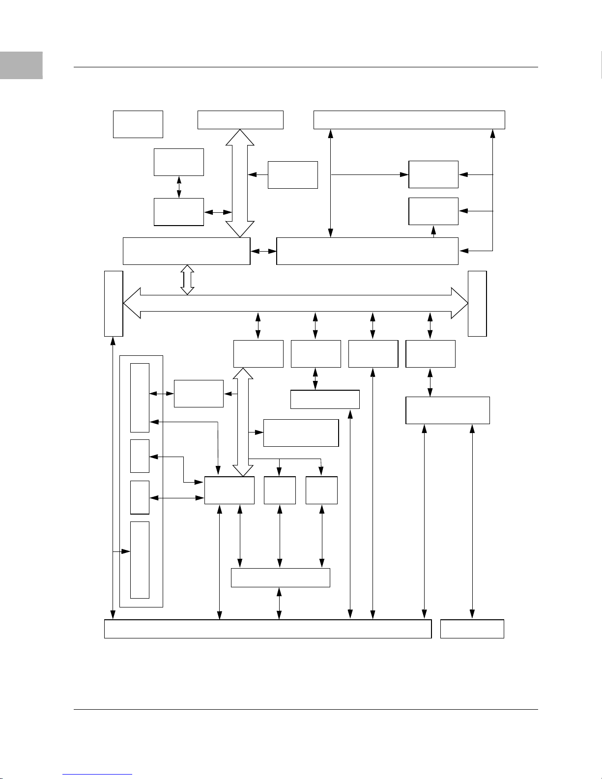
The block diagram in Figure 1-1 illustrates the architecture of the
MVME2700 base board. For a view of the overall boa rd architectu re, refer
to Figure 5-1 in the Functional Description chapter.
1-1
Page 15
1
Introduction to the MVME2700
CLOCK
GENERATOR
64-BIT PMC SLOT
L2 CACHE
1MB
PROCESSOR
MPC750
PHB & MPIC
RAVEN ASIC
ISA
REGISTERS
FLASH
1MB
PROCESSOR BUS
MEMORY CONTROLLER
FALCON CHIPSET
33MHz 32/64-BIT PCI LOCAL BUS
PIB
W83C553
ETHERNET
DEC21140
AUI/10BT/100BTX
MEMORY EXPANSION CONNE CTORSDEBUG CONNECTOR
SCSI
53C825A
FLASH
4MB or 8MB
SYSTEM
REGISTERS
PCI EXPANSION
VME BRIDGE
UNIVERSE II
BUFFERS
RTC/NVRAM/WD
ISA BUS
SUPER I/O
PC87308
MOUSE KBD FLOPPY & LED
SERIAL
PARALLEL
712/761 P2 I/O OPTIONS
PMC FRONT I/O SLOT
FRONT PANEL
VME P2 VME P1
ESCC
85230
M48T559
CIO
Z8536
Figure 1-1. MVME2700 Base Board Block Diagram
1-2 Computer Group Literature Center Web Site
Page 16

Equipment Required
The following equipment is required to complete an MVME2700 system:
❏ VME syst em enclosure
❏ System console terminal
❏ Operating system (and/or application software)
❏ Disk drives (and/or other I/O) and controllers
❏ Transition module (MVME712M or MVME761) and connecting
cables
MVME2700 VMEmodules are factory-configured for I/O handling via
either MVME712M or MVME761 transition modules. The following
table shows the r elationship be tween MVME2700 model numbers and th e
applicable transition module.
Equipmen t Required
1
Table 1-1. VMEmodule/Transition Module Correspondence
MVME761-Compatible Models* MVME712-Compatible Models*
MVME2700-1221A (16MB ECC DRAM) MVME2700-4221A (16MB ECC DRAM)
MVME2700-1231A (32MB ECC DRAM) MVME2700-4231A (32MB ECC DRAM)
MVME2700-1241A (64MB ECC DRAM) MVME2700-4241A (64MB ECC DRAM)
MVME2700-1251A (128MB ECC DRAM) MVME2700-4251A (128MB ECC DRAM)
MVME2700-1321 (16MB ECC DRAM MVME2700-4321 (16MB ECC DRAM)
MVME2700-1331 (32MB ECC DRAM) MVME2700-4331 (32MB ECC DRAM)
MVME2700-1341 (64MB ECC DRAM) MVME2700-4341 (64MB ECC DRAM)
MVME2700-1351 (128MB ECC DRAM) MVME2700-4351 (128MB ECC DRAM)
MVME2700-1361 (256MB ECC DRAM) MVME2700-4361 (256MB ECC DRAM)
MVME2700-1421 (16MB ECC DRAM) MVME2700-4421 (16MB ECC DRAM)
MVME2700-1431 (32MB ECC DRAM) MVME2700-4431 (32MB ECC DRAM)
MVME2700-1441 (64MB ECC DRAM) MVME2700-4441 (64MB ECC DRAM)
MVME2700-1451 (128MB ECC DRAM) MVME2700-4451 (128MB ECC DRAM)
MVME2700-1461 (256MB ECC DRAM) MVME2700-4461 (256MB ECC DRAM)
MVME2700-3221A (16MB ECC DRAM)
MVME2700-3231A (32MB ECC DRAM)
http://www.mcg.mot.com/literature 1-3
Page 17

1
Introduction to the MVME2700
Table 1-1. VMEmodule/Transition Module Correspondence
MVME761-Compatible Models* MVME712-Compatible Models*
MVME2700-3241A (64MB ECC DRAM)
MVME2700-3251A (128MB ECC DRAM)
MVME2700-3321 (16MB ECC DRAM)
MVME2700-3331 (32MB ECC DRAM)
MVME2700-3341 (64MB ECC DRAM)
MVME2700-3351 (128MB ECC DRAM)
MVME2700-3361 (256MB ECC DRAM)
MVME2700-3421 (16MB ECC DRAM)
MVME2700-3431 (32MB ECC DRAM)
MVME2700-3441 (64MB ECC DRAM)
MVME2700-3451 (128MB ECC DRAM)
MVME2700-3461 (256MB ECC DRAM)
*All model s have 233MHz, 266M Hz o r 366M H z pro ces sor s, 5MB or 8M B Fl ash mem or y
and 1MB L2 cache.
In models of the MVME2700 series that are co nfigured for MVME712M
I/O mode, the pin assignments of VMEbus connector P2 are fully
compatible with other transition modules of the MVME712 series. In
MVME761-compatible models, certain signals are multiplexed through
P2 for additional I/O capacity. Refer to P2 Signal Mu ltiple x ing in Chapter
5 for details.
1-4 Computer Group Literature Center Web Site
Page 18

Overview of Startup Procedure
Overview of Startup Procedure
The following tabl e lists t he things you wil l need to d o before you ca n use
this board and tells where to find the information yo u need to per form each
step. Be sure to r ead this entir e chapter, in cluding all Caut ion and Warning
notes, before you begin.
Table 1-2. Startup Overview
What you need to do... Refer to... On page...
Unpack the hardware. Unpacking Instructions 1-6
1
Configure th e hardware by setting
jumpers on the boards and
transition modules.
Ensure that mezzanine boards are
properly instal led.
Install the MVME2700
VMEmodule in the chassis.
Install the transition modul e in th e
chassis.
Connect a console termina l. System Considerations, MVME2700 VMEmodule 3-17
Connect any othe r equipment you
will be using.
Power up the system. Applying Power 4-1
Note that the debugger initializ es
the MVME2700.
MVME2700 Base Board Preparation and
MVME712M Transition Module Preparation or
MVME761 Transition Module Preparation
Hardware Inst allation, RAM200 Memory Mezzanine;
PMC Module; PMC Carrier Board
MVME2700 VMEmodule Installa tio n 3-9
MVME712M Transition Module Installation or
MVME761 Transition Module Installation
Connector Pin Assignments
For more information on optional devices and
equipment, refer to the documentation provided with
the equipment.
Troubleshooting CPU Boards; Solving Start-Up
Problems
Using the Debugger 7-3
You may also wish to obtain the PPCBu g Firmware
User’s Manual, listed in Appendix A, Related
Documentation.
2-2 and
2-8 or 2-18
3-3
through
3-6
3-11
or 3-14
6-1
D-1
A-1
Initialize the system clock. Using the Debugger, Debugger Commands 7-3
Examine and/or change
environmental parameters.
Program the board as needed for
your applicati ons.
http://www.mcg.mot.com/literature 1-5
Using PPCBug Firmware, Displaying the Board
Configuration Block
CNFG and ENV commands 8-2
7-3
and/or 8-1
Page 19

1
Introduction to the MVME2700
Unpacking Instructions
Note If the shipping carton is damaged upon receipt, request that
the carrier’s agent be present during the unpacking and
inspection of the equipment.
Unpack the equipment from the shipping carton. Refer to the packing list
and verify t hat all items are pr es ent . Sa ve t he packing materia l for storing
and reshipping of equipment.
Avoid touching areas of integrated circuitry; static discharge
!
Caution
can damage circuits.
Hard ware Co nfiguration
To produce the desired configuration and ensure proper operation of the
MVME2700, you may need to carry out certain hardware modifications
before installing the module.
The MVME2700 provides software control over most options: by setting
bits in control registers after installing the module in a system, you can
modify its confi gurat ion. The M VME27 00 contr ol regi ster s are de scrib ed
in Chapter 5, and/or in the MVME2600 Series Single Board Computer
Programmer’s Reference Guide listed under Related Documentation.
Some options, however, ar e not software-programma ble. Such options are
controlled through manual installation or removal of header jumpers or
interface modules on the base board or the associated transition module.
Instructions on preparing the base board, transition modules and P2
adapter are covered in Chapter 2. Installation instructions for the base
board, memory mezzanine , transition modu les and P2 adapter are c overed
in Chapter 3.
1-6 Computer Group Literature Center Web Site
Page 20

Overview
The following sections discuss the:
Covered in this chapter is information on the c onfigurable items on the
MVME2700 base board and MVME712M and MVME761 transition
modules and their ser ia l port se tting s and confi gurat ion s. The P2 adapte rs
(three- and five-r ow) us ed wit h the tra nsi ti on modul es are also described.
2Hardware Preparation
2
❏ Preparation of the MVME2700 base board, including jumper
settings
❏ Preparation of the MVME712M and MVME761transition modules
❏ Preparat ion of the P 2 adapter card
2-1
Page 21

Hardware Preparation
2
MVME2700 Base Board Preparation
Figure 2-1 illustrates the placement of the swi tches, jumper header s,
connectors, and LED indicators on the MVME2700. Manually
configurable i tems on the base board are lis ted in the following table . Refer
to the sections or figures listed along side the jumper function for more
information.
Table 2-1. Jumper Settings
Jumper Function
J9 Flash bank selection, page 2-4
J20 System controller sel ec ti on, pa ge 2-7
J18 SP3 transmit clock configurat ion , page 2-6
J16 SP4 receive cl ock config ur ation, page 2-4
J17 SP4 transmit clock configurat ion , page 2-5
J19 SP4 transmit clock receiver buffer control, page 2-5
In conjunction with the serial port settings on the base board, serial ports
on the associated MVME712M or MVME761 transition module are also
manually configurable. For a discussion of the configurable items on the
transition module, refer to the MVME712M Transition Module
Prep aration and MVME761 Transition Module Preparation sections. For
further information, refer to the Related Documentation appendix.
The MVME2700 is factory tested and shipped with the configurations
described in the following sections. The MVME2700’s required and
factory-installed debug monitor, PPCBug, operates with those factory
settings.
2-2 Computer Group Literature Center Web Site
Page 22

MVME2700 Base Board Preparation
.
2
2
1
J1
14
13
252449
ABT
RST
FLOPPY/LED
50
U8
189
190
J2
BATTERY
J3
CHS
BFL
CPU
PCI
FUS
SYS
KEYBOARD
MOUSE
27
2
26
F1
4
2
1
3
4
2
1
3
89
90
1
J6
6
J5
5
65
J7
2
1
30
4
5
29
XU1 XU2
13
5
13
21
20
14
30
4
29
21
20
14
1
2
Z1
A1
B1
C1
P1
C32D1D32
Z32
A32
B32
2
1
F2
J4
114
113
Z1A1B1
C1
F3
2
2
1
1
J12
J11
PCI MEZZANINE CARD
2
1
J8
16
15
J8 and J10 connectors are unpopulated
3
1
J9
1
8
J10
64
63
1
J13
63
3
1
3
1
3
1
J16
J17
1
J18
2
J19 J20
64
63
2
1
2
J14
64
63
64
3
1
P2
C32D1D32
Z32
A32
B32
11865.00 9709
Figure 2-1. MVME2700 Switches, Headers, Connectors, Fuses, LEDs
http://www.mcg.mot.com/literature 2-3
Page 23

Hardware Preparation
2
Flash Bank Selection (J9)
The MVME2700 base board has provision for 1MB of 16-bit Flash
memory. The RAM200 memory mezzanine acc ommodates 4MB or 8MB
of additional 64-bit Flash memory.
The Flash memory is organized in either one or two banks, each bank
either 16 or 64 bits wide.
To enable Flash bank A (4MB or 8MB of firmware resident on solderedin devices on the RAM200 mezzanine), place a jumper across header J9
pins 1 and 2. To enable Flash bank B (1MB of firm ware located in soc kets
on the base board), place a jumper across header J9 pins 2 and 3.
3
2
1
J9J9
3
2
1
Flash Bank A Enabled (4MB/8MB, Soldered)
Flash Bank B Enabl ed (1MB, Socket s)
(factory configuration)
Serial Port 4 Receive Clock Configuration (J16)
In synchronous serial communicatio ns, you can configure se ri al port 4 on
the MVME2700 to use the cl ock si gnals provided by the RxC sign al l in e.
The configurations for the MVME712M-compatible and MVME761compatible versions of the base board require different settings for port 4
to either d rive or receive RxC (default).
J16
3
2
1
Drive RxC
J16
3
2
1
Receive RxC
(factory configuration)
2-4 Computer Group Literature Center Web Site
Page 24

MVME2700 Base Board Preparation
Serial port configurations for the MVME712M are illustrated in figures
2-4 through 2-9.
Serial port co nfigurations f or the MVME761 are il lustrated in f igures 2- 11
through 2-28.
Serial Port 4 Transmit Clock Configuration (J17)
In synchronous serial communicatio ns, you can configure se ri al port 4 on
the MVME2700 to use the clock signals provided by the TxC signal line.
Header J17 configures port 4 to ei ther dr ive or re ceive TxC (defaul t). The
factory configuration has port 4 set to receive TxC.
A complete configuration of serial port 4 requires that you set additional
jumper headers on the MVME2700 or the transition module.
J17J17
3
2
3
2
2
1
Drive TxC
1
Receive TxC
(factory configuration)
Serial port configurations for the MVME712M are illustrated in figures
2-4 through 2-9.
Serial port co nfigurations f or the MVME761 are il lustrated in f igures 2- 11
through 2-28.
Serial Port 4 Transmit Clock Receiver Buffer Control (J19)
A transmit clock receiver buffer (controlled by header J19) is associated
with serial port 4. Inst alling a ju mper on J19 enables t he buffer. Removing
the jumper dis ables the buffer. The factory con figuration has th e serial port
4 buffer enabled.
http://www.mcg.mot.com/literature 2-5
Page 25

Hardware Preparation
2
As described in other sections, a complete configuration of serial port 4
requires that you set additional jumper heade rs on t he MVME2 700 or t he
transition module.
J19
2
1
Buffer Enabled
(factory configuration)
J19
2
1
Buffer Disabled
Serial port configurations for the MVME712M are illustrated in figures
2-4 through 2-9.
Serial port co nfigurations f or the MVME761 are il lustrated in f igures 2- 11
through 2-28.
Serial Port 3 Transmit Clock Configuration (J18)
On MVME761-compatible versions only of the base board, this header
configures port 3 to ei ther drive or rec eive TxC. The factory conf iguration
has serial port 3 set to receive TxC. On MVME761-compatible versions,
you must set J2 on the transition module to c o mple te the configuration of
serial port 3.
J18J18
3
2
1
Drive TxC
3
2
1
Receive TxC
(factory configuration)
Serial port configurations for the MVME712M are illustrated in figures
2-4 through 2-9.
Serial port co nfigurations f or the MVME761 are il lustrated in f igures 2- 11
through 2-28.
2-6 Computer Group Literature Center Web Site
Page 26

MVME2700 Base Board Preparation
System Controller Sel ection (J20)
The MVME2700 is factory-c onfigured as a VMEbus sys tem controller by
jumper header J20. If you select the “automatic” system controller
function by placing a jumper on J20 pins 2 and 3, the MVME2700
determines wheth er it is t he system cont roller by its posi tion on the b us. If
the board is in the fi rs t sl ot from the left, it configures itself as the system
controller. If the MVME2700 is not to be system controller under any
circumstances, place the jumper on J20 pins 1 and 2. When the board is
functioning as system controller, the
J20
3
2
1
Not System Controller
Auto System Controller
J20
3
2
1
(factory configuration)
2
SCON LED is turned on.
J20
3
2
1
System Controller
Remote Status and Control (J1)
The MVME2700 front panel LEDs and switches are mounted on a
removable mezzanine board. Removing the LED mezzanine makes the
mezzanine connect or (J1, a keyed, double-row 14-pin con nector) available
for service as a remote sta tus and cont rol connect or. In thi s applica tion, J1
can be connected to a user-supplied external cable to carry the Reset and
Abort signals and the LED lines to a control panel located apart from the
MVME2700. Maximum cable length is 15 feet.
Table 6-1 lists the pin numbers and signal mnemonics for J1.
http://www.mcg.mot.com/literature 2-7
Page 27

Hardware Preparation
2
MVME712M Transition Module Preparation
The MVME712M transition module and P2 adapter board are used in
conjunction with the following models of the MVME2700 VMEmodule:
With MCG front panel/handles With Scanbe front panel/handles
MVME2700-4321 (16MB ECC DRAM) MVME2700-4221A (16MB ECC DRAM)
MVME2700-4331 (32MB ECC DRAM) MVME2700-4231A (32MB ECC DRAM)
MVME2700-4341 (64MB ECC DRAM) MVME2700-4241A (64MB ECC DRAM)
MVME2700-435 1 (128MB ECC DRAM) MVME2700-4251A (128MB ECC DRA M)
MVME2700-4361 (256MB ECC DRAM) MVME2700-4421 (16MB ECC DRAM)
MVME2700-4431 (32MB ECC DRAM)
MVME2700-4441 (64MB ECC DRAM)
MVME2700-4451 (128MB ECC DRAM)
MVME2700-4461 (256MB ECC DRAM)
For a description of the MVME712M features, refer to MVME712M
Transition Module on page 5-24.
For installation s in VME64 backplanes, you may wish to use the five- row
P2 adapter and cable supplied with the MVME761 transition module.
Although the MVME712M itself does not support the additional I/O
capability on rows D and Z of the MVME2700’s five-row P2 connector,
those signals remain available for user-specific applications. To gain
access to the 16-bit SCSI and PMC I/O present on rows D and Z when the
MVME2700 is installed in a VME64 backplane, use the five-row P2
adapter.
2-8 Computer Group Literature Center Web Site
Page 28

MVME712M Transition Module Preparation
MVM E712M
SERIAL PORT 3
SERIAL PORT 4
ETHERNET
2
2
SERIAL PORT 1 /CONSOLE
1
132513
25
J7
J9
14
1141
13
1
J15
1
212
13
1
SERIAL PORT 2 / TTY
132513
25
11
J10
J8
14
1141
13
1
PRIMAR Y SIDE
13
INTERFACE
SCSI
J6
DS2DS1
2
1
J1
J11
14
13
14
2
2
1
J13
J14
2
14
13
2
1
J16
13
14
2
1
J18
13
14
1
14
2
J17
14
2
J19
14
J20
20
19
16
J21
A1
C1 C32
2
1
C1 C2 C3
J2
J3
PRINTER
915
18
49
50
R49
81
18 1
36
J4
R50
81
R51
19
J5
cb228 9212
81
1
2
A32
50
49
Figure 2-2. MVME712M Connector and Header Locations
http://www.mcg.mot.com/literature 2-9
Page 29

Hardware Preparation
2
Serial Ports 1-4 DCE/DTE Configuration
Serial ports 1 t hrough 4 are conf igurable as modems (DCE) for connectio n
to termina ls, or as term inals (DTE) f or connection to modems. The
MVME712M is shipped with the serial ports configured for DTE
operation. Serial port DCE/DTE configuration is accomplished by
positioning jumpers on one of two headers per port. The following table
lists the serial ports with their corresponding jumper headers.
Table 2-2. MVME712M Port/Jumper Correspondence
Serial Port
Port 1 J7 Serial port 1/ Console
Port 2 J8 Serial port 2/ TTY
Port 3 J9 Serial port 3
Port 4 J10 Serial port4
Figures 2-4 through 2-9 illustrate the MVME2700 base board and
MVME712M transition module with the interconnections and jumper
settings for DCE/DTE configuration on each serial port.
Board
Connector
Panel Connector
Jumper Header
DCE/DTE
J1/J11
J16/J17
J13/J14
J18/J19
Serial Port 4 Clock Configuration
Serial port 4 can be configured via J15 (Figure 2-3) to use the TrxC4 and
RtxC4 signal lines. Pa rt of the configurat ion is done with heade rs J16, J17,
and J19 on the MVME2700 (Figures 2-8 and 2-9).
J15
31 957 11
TRXC4 TO PORT 4 PIN 15
TRXC4 TO PORT 4 PIN 17
TRXC4 TO PORT 4 PIN 24
Figure 2-3. J15 Clock Line Configuration
2-10 Computer Group Literature Center Web Site
RTXC4 TO PORT 4 PIN 24
RTXC4 TO PORT 4 PIN 17
RTXC4 TO PORT 4 PIN 15
Page 30

MVME2700 SERIES
VME MODULE
P2 ADAPT ER
BOARD
MVME712M Transition Module Preparation
64-PIN
CABLE
MVME712M
MODULE
2
DCE
PC87308
SOUT1
RTS1#
DTR1#
SIN1
CTS1#
DCD1#
DSR1#
RI1#
MVME2700 SERIES
VME MODULE
PC87308
SOUT1
NC
NC
NC
NC
P2 ADAPTER
BOARD
64-PIN
CABLE
RXD
3
CTS
5
+12V
+12V
DCD
TXD
RTS
DSR
GND
8
2
4
6
7
DB25
CONNECTOR
Install all jumpers on J1
Remove all jumpers on J11
11551.00 9609 (1-8)
MVME712M
MODULE
TXD
11551.00 9609 (2-8)
2
RTS
DTR
RXD
CTS
GND
4
20
3
5
7
DB25
CONNECTOR
DTE
RTS1#
DTR1#
SIN1
CTS1#
DCD1#
DSR1#
RI1#
NC
NC
NC
NC
+12V
In st a ll a ll ju mp e rs o n J 1 1
Rem ove all jum pers on J1
Figure 2-4. MVME712M Serial Port 1 DCE/DTE Configuration
http://www.mcg.mot.com/literature 2-11
Page 31

2
Hardware Preparation
MVME2700 SERIES
VME MODULE
P2 ADAPTER
BOARD
64-PIN
CABLE
MVME712M
MODULE
DCE
PC87308
SOUT2
RTS2#
DTR2#
SIN2
CTS2#
DCD2#
DSR2#
RI2#
MVME2700 SERIES
VME MODULE
NC
NC
P2 ADAPTER
BOARD
64-PIN
CABLE
+12V
RXD
DCD
DTR
DSR
GND
CTS
TXD
RTS
3
5
8
2
4
20
6
7
DB25
CONNECTOR
Install all jumpers on J16
Remove all jumpers on J17
11551.00 9609 (3-8)
11551.00 9609 (4-8)
MVME712M
MODULE
DTE
PC87308
TXD
RTS
DTR
CTS
2
4
20
3
5
8
7
DB25
CONNECTOR
SOUT2
RTS2#
DTR2#
SIN2
CTS2#
DCD2#
DSR2#
RI2#
NC
NC
RXD
DCD
GND
Install all jumpers on J17
Remove all jum pers on J16
Figure 2-5. MVME712M Serial Port 2 DCE/DTE Configuration
2-12 Computer Group Literature Center Web Site
Page 32

Z85230
MVME2700 SERIES
VME MODULE
TXDA
P2
ADAPTER
MVME712M Transition Module Preparation
64-PIN
CABLE
MVME712M
MODULE
RXD
3
2
DCE
RTSA#
DCDA#
RXDA
CTSA#
TRXCA#
RTXCA#
Z8536
DTR3#
LLB3#
RLB3#
DSR3#
RI3#
TM3#
NC
NC
NC
NC
NC
NC
NC
+12V
CTS
DTR
TXD
RTS
DCD
DSR
GND
5
20
2
4
DB25
CONNECTOR
8
6
7
Header J18 is open
Figure 2-6. MVME712M Serial Port 3 DCE Configuration
http://www.mcg.mot.com/literature 2-13
Install all jumpers on J13
Remove all jumpers on J14
11551.00 9609 (5-8)
Page 33

2
Hardware Preparation
MVME2700 SERIES
VME MODULE
Z85230
TXDA
P2
ADAPTER
64-PIN
CABLE
MVME712M
MODULE
TXD
2
DTE
RTSA#
DCDA#
CTSA#
TRXCA#
RTXCA#
Z8536
DTR3#
LLB3#
RLB3#
DSR3#
RXDA
NC
NC
NC
NC
NC
RTS
DCD
RXD
CTS
DTR
4
8
3
5
DB25
CONNECTOR
20
RI3#
TM3#
Header J18 is open
NC
NC
GND
7
Install all jumpers on J14
Remove all jumpers on J13
11551.00 9609 (6-8)
Figure 2-7. MVME712M Serial Port 3 DTE Configuration
2-14 Computer Group Literature Center Web Site
Page 34

MVME712M Transition Module Preparation
2
DTE
MVME2700 SERIES
VME MODULE
Z85230
TXDB
RTSB#
DCDB#
RXDB
CTSB#
TRXCB
RTXCB
Z8536
DTR4#
LLB4#
J19
NC
J17
J16
P2
ADAPTER
1
2
3
1
2
3
64-PIN
CABLE
MVME712M
MODULE
J15
TXD
RTS
DCD
RXD
CTS
TXCI
RXCI
TXCO
DCD
2
4
8
3
5
15
17
24
20
DB25
CONNECTOR
RLB4#
DSR4#
Headers:
RI4#
TM4#
J16 2-3
J17 2-3
NC
NC
NC
NC
Install all jumpers on J18
Remove all jumpers on J19
J19 1-2
NOTE: No jumpers on J15. Refer to Figure 2-3 on pa ge 2-10.
Figure 2-8. MVME712M Serial Port 4 DCE Configuration
GND
7
11551.00 9609 (7-8)
http://www.mcg.mot.com/literature 2-15
Page 35

2
Hardware Preparation
MVME2700 SERIES
VME MODULE
Z85230
TXDB
P2
ADAPTER
64-PIN
CABLE
MVME712M
MODULE
TXD
2
DTE
RTSB#
DCDB#
CTSB#
TRXCB
RTXCB
Z8536
DSR4#
RXDB
DTR4#
LLB4#
RLB4#
J19
NC
NC
NC
J17
J16
RTS
4
DCD
8
RXD
3
CTS
5
1
2
3
1
2
3
J15
TXCI
RXCI
TXCO
DCD
15
17
24
20
DB25
CONNECTOR
NC
NC
GND
7
Install all jumpers on J19
Remove all jumpers on J18
11551.00 9609 (8-8)
Headers:
RI4#
TM4#
J16 2-3
J17 2-3
J19 1-2
NOTE: No jumpers on J15. Refer to Figure 2-3 on pa ge 2-10.
Figure 2-9. MVME712M Serial Port 4 DTE Configuration
2-16 Computer Group Literature Center Web Site
Page 36

MVME712M Transition Module Preparation
P2 Adapter Preparation
In its factory configuration, the MVME712M transition module uses a
three-row P2 adapter to transfer synchronous/asynchronous serial,
parallel, and Ethernet signals to and from the MVME2700 series
VMEmodule. A 50-pin male connector (J 3) on the P2 ad apter carries 8-bit
SCSI signals from the MVME2700.
Preparation of the three-row P2 adapter for the MVME712M consists of
removing or installing the SCSI termin ating resi stors, R1- R3. Figure 2- 10
illustrates the location of the resistors, the co nnectors, and SCSI t erminator
power fuse F1. For further infor mation on the preparatio n of the transition
module and this P2 adapter, refer to the user’s manual for the
MVME712M, listed in Related Documentation.
A1
B1
C1
2
1
J2
J3
A32
B32
C32
50
49
2
1
2
1
C1 C2 C3 F1
C1
B1
A1
R2 R3R1
CR1
C32
B32
A32
P2
cb211 9212
Figure 2-10. MVME712M Three-Row P2 Adapter
If you plan to connect the MVME712M to a VME64 backplane with a
five-row P2 adapter refer to on page 2-27 for guidelines on preparing the
adapter.
http://www.mcg.mot.com/literature 2-17
Page 37

Hardware Preparation
2
MVME761 Transition Module Preparation
The MVME761 transiti on module (Figu re 2-11) and P2 adapt er board are
used in conjunction with the following models of the MVME2700
VMEmodule:
MCG front panel/handles Scanbe front panel handles
MVME2700-1221A (16MB ECC DRAM) MVME2700-3221A (16MB ECC DRAM)
MVME2700-1231A (32MB ECC DRAM) MVME2700-3231A (32MB ECC DRAM)
MVME2700-1241A (64MB ECC DRAM) MVME2700-3241A (64MB ECC DRAM)
MVME2700-1251A (128MB ECC DRAM) MVME2700-3251A (128MB ECC DRAM)
MVME2700-1321 (16MB ECC DRAM) MVME2700-3 421 (16MB ECC DRAM)
MVME2700-1331 (32MB ECC DRAM) MVME2700-3 431 (32MB ECC DRAM)
MVME2700-1341 (64MB ECC DRAM) MVME2700-3 441 (64MB ECC DRAM)
MVME2700-1351 (128MB ECC DRAM) MVME2700-3 451 (128MB ECC DRAM)
MVME2700-1361 (256MB ECC DRAM) MVME2700-3 461 (256MB ECC DRAM)
MVME2700-1421 (16MB ECC DRAM)
MVME2700-1431 (32MB ECC DRAM)
MVME2700-1441 (64MB ECC DRAM)
MVME2700-1451 (128MB ECC DRAM)
MVME2700-1461 (256MB ECC DRAM)
MVME2700-3321 (16MB ECC DRAM)
MVME2700-3331 (32MB ECC DRAM)
MVME2700-3341 ( 64MB ECC DRAM)
MVME2700-3351 12 8MB ECC DRAM)
MVME2700-3361 (256MB ECC DRAM)
For a description of the MVME761M features, refer to MVME761
Transition Module on page 5-25.
Use the MVME761’s three-row P2 adapter board in three-row VME
backplanes. Use the five-row adapter in VME64 backplanes, which are
equipped with five-row P2 connectors.
2-18 Computer Group Literature Center Web Site
Page 38

MVME
761-001
J5
J6
DTE
MVME761 Transition Module Preparation
2
DCE
J2
1
3
1910 9609
SERIAL 3COM1 COM2 PARALLEL
60
59
J1
2
1
J7
J8
60
59
DTE
1 3
J12
DCE
J3
J4
10/100 BASETSERIAL 4
2
1
P2
J9
Figure 2-11. MVME761 Connector and Header Locations
http://www.mcg.mot.com/literature 2-19
Page 39

Hardware Preparation
2
Serial Ports 1 and 2
On MVME761-compatible models of the MVME2700, th e asynch ronous
serial ports (serial ports 1 and 2) are configured permanently as Data
Circuit-terminating Equipment (DCE). The port configuration is
illustrated in Figure 2-12.
Configuration of Serial Ports 3 and 4
The synchronous serial ports, serial port 3 and serial port 4, are
configurable thr oug h a combin at ion of serial interface module (SI M)
selection and jumper settings . The following tabl e lists the SIM connectors
and jumper head ers cor respo nding to eac h of the s ynchro nous ser ia l port s.
Synchronous Port Board Connector SIM Connector Jumper
Header
Port 3 J7 J1 J2
Port 4 J8 J12 J3
Serial port 3 is r outed to board con nector J7. Serial por t 4 is routed to boar d
connector J8. Eight serial interface modules are available:
❏ EIA-232-D (DCE and DTE)
❏ EIA-530 (DCE and DTE)
❏ V.35 (DCE and DTE)
❏ X.21 (DCE and DTE)
You can configure ser ial ports 3 and 4 for an y of the above serial pr otocols
by installing the appropriate serial interface module and setting the
corresponding jumper. Refer to Figure 2-12 on page 2-22 through Figure
2-28 on page 2-38. SIMs can be ordered separately as required.
Note Part numbers of the various SIMs are listed in
Table 5-6 on page 5-26, SIM Type Identifica ti on.
2-20 Computer Group Literature Center Web Site
Page 40

MVME761 Transition Module Preparation
Headers J2 and J3 are used to configure serial port 3 and serial port 4,
respectively, in tandem with SIM selection. With the jumper in position
1-2, the port is configured as a DTE. With the jumper in position 2-3, the
port is configured as a DCE. The jumper setting of the port should match
the configuration of the corresponding SIM module.
J2
123
DCE DTE
J3
123
DCE DTE
J2
Serial Port 3 jumper settings
123
J3
Serial Port 4 jumper settings
123
2
When installing the SIM modules, note that the headers are keyed for
proper orientation.
For further information on the preparation of the transition module, refer
to the user’s manual for the MVME761 , listed in Related Documentation.
The next figures illustrate the MVME2700 base board and MVME761
transition module with the interco nnections and jumper set tings for
DCE/DTE configuration on each serial port.
http://www.mcg.mot.com/literature 2-21
Page 41

2
Hardware Preparation
DCE
MVME2700 SERIES
SOUT1
RTS1#
DTR1#
SIN1
CTS1#
DSR1#
DCD1#
RI1#
PC87308
SOUT2
RTS2#
DTR2#
P2/P2MX
MVME761
DB9
3
7
4
2
8
6
1
9
5
DB9
3
7
4
COM1
CONNECTOR
SIN2
CTS2#
DSR2#
DCD2#
RI2#
11552.00 9802 (1-5)
2
COM2
8
CONNECTOR
6
1
9
5
Figure 2-12. MVME761 Serial Ports 1 and 2 (DCE Only)
2-22 Computer Group Literature Center Web Site
Page 42

MVME761 Transition Module Preparation
2
DCE
VME MODULE
Z85230 SCC
RTS#
RXD
CTS#
DCD#
TRXC
RTXC
Z8536 CIO
DTR#
LLB#
RLB#
TXD
J18
3
2
1
P2/P2MX
MVME761
EIA232-DCE SIM
J2
3
2
1
HD26
3
5
2
4
20
15
17
24
8
25
22
DSR#
RI#
TM#
6
21
18
7
Header J18 1-2 Header J2 2-3
11552 9902 (2-5)
Figure 2-13. MVME761 EIA-232-D Port 3 DCE Configuration
http://www.mcg.mot.com/literature 2-23
Page 43

2
Hardware Preparation
DTE
VME MODULE
Z85230 SCC
TXD
RTS#
RXD
CTS#
DCD#
TRXC
RTXC
Z8536 CIO
DTR#
LLB#
RLB#
J18
3
2
1
P2/P2MX
MVME761
EIA232-DTE SI M
J2
3
2
1
HD26
2
4
3
5
8
24
15
17
20
18
21
DSR#
RI#
TM#
6
22
25
7
Header J18 2-3 Header J2 1-2
11552 9902(4-5 )
Figure 2-14. MVME761 EIA-232-D Port 3 DTE Configuration
2-24 Computer Group Literature Center Web Site
Page 44

MVME761 Transition Module Preparation
2
DCE
Z85230 SCC
RTS#
RXD
CTS#
DCD#
TRXC
RTXC
Z8536 CIO
DTR#
LLB#
VME MODULE
TXD
J19
J16
1
2
3
1
2
3
P2/P2MX
MVME761
EIA232-DCE SI M
J3J17
3
2
1
HD26
3
5
2
4
20
15
17
24
8
25
RLB#
DSR#
RI#
TM#
22
6
21
18
7
Headers: J16 2-3 Header J3 2-3
J17 1-2
J19 1-2
11552 9902 (3-5)
Figure 2-15. MVME761 EIA-232-D Port 4 DCE Configuration
http://www.mcg.mot.com/literature 2-25
Page 45

2
Hardware Preparation
DTE
Z85230 SCC
RTS#
RXD
CTS#
DCD#
TRXC
RTXC
Z8536 CIO
DTR#
LLB#
VME MODULE
TXD
J19
J16
1
2
3
1
2
3
P2/P2MX
MVME761
EIA232-DTE SIM
J3J17
3
2
1
HD26
2
4
3
5
8
24
15
17
20
18
RLB#
DSR#
RI#
TM#
Headers: J16 2-3
Header J3 1-2
21
6
22
25
7
J17 2-3
J19 1-2
11552 9902 (5-5)
Figure 2-16. MVME761 EIA-232-D Port 4 DTE Configuration
2-26 Computer Group Literature Center Web Site
Page 46

MVME761 Transition Module Preparation
2
DCE
VME MODULE
Z85230 SCC
RTS#
RXD
CTS#
DCD#
TRXC
RTXC
Z8536 CIO
DTR#
LLB#
RLB#
DSR#
TXD
RI#
TM#
J18
3
2
1
P2/P2MX
MVME761
EIA530-DCE SIM
+
+
+
-
3
2
1
J2
+
-
+
+
-
-V
-V
RXDB
RXDA
CTSB
CTSA
TXDB
TXDA
RTSB
RTSA
DTRB
DTRA
TXCB
TXCA
RXCB
RXCA
ETXCB
ETXCA
DCDB
DCDA
TM
RI
DSRB
DSRA
RL
LL
GND
DB25
16
3
13
5
14
2
19
4
23
20
20
12
15
15
9
17
17
11
24
10
8
25
26
22
6
21
18
7
Figure 2-17. MVME761 EIA-530-DCE Configuration Por t 3
http://www.mcg.mot.com/literature 2-27
Header J2 2-3Header J18 1-2
2191 9902
Page 47

2
Hardware Preparation
DTE
VME MODULE
Z85230 SCC
RTS#
CTS#
DCD#
TRXC
RTXC
Z8536 CIO
DTR#
LLB#
RLB#
DSR#
TXD
RXD
RI#
TM#
J18
3
2
1
P2/P2MX
3
2
1
J2
MVME761
EIA530-DTE SI M
+
+
+
-
+
-
+
+
-
+
-
-V
-V
TXDB
TXDA
RTSB
RTSA
RXDB
RXDA
CTSB
CTSA
DTRB
DTRA
ETXCB
ETXCA
TXCB
TXCA
RXCB
RTXCA
DTRB
DTRA
LL
RL
DSRB
DSRA
(RI)
TM
GND
DB25
14
2
19
4
16
3
13
5
10
8
11
24
12
15
9
17
23
20
18
21
22
6
26
25
7
Figure 2-18. MVME761 EIA-530-DTE Configuration Port 3
2-28 Computer Group Literature Center Web Site
Header J2 1-2Header J18 2-3
2194 9902
Page 48

MVME761 Transition Module Preparation
2
DCE
Z85230 SCC
RTS#
RXD
CTS#
DCD#
TRXC
RTXC
Z8536 CIO
DTR#
LLB#
RLB#
DSR#
VME MODULE
TXD
RI#
TM#
J19
J17
J16
1
2
3
1
2
3
P2/P2MX
MVME761
EIA-530 DCE SI M
+
-
+
-
+
-
3
2
1
J3
+
-
+
+
-
-V
-V
RXDB
RXDA
CTSB
CTSA
TXDB
TXDA
RTSB
RTSA
DTRB
DTRA
TXCB
TXCA
RXCB
RXCA
ETXCB
ETXCA
DCDB
DCDA
TM
RI
DSRB
DSRA
RL
LL
GND
DB25
16
3
13
5
14
2
19
4
23
20
20
12
15
15
9
17
17
11
24
10
8
25
26
22
6
21
18
7
J17 1-2
J19 1-2
Figure 2-19. MVME761 EIA-530-DCE Configuration Por t 4
http://www.mcg.mot.com/literature 2-29
Header J3 2-3Headers: J16 2-3
2197 9804
Page 49

2
Hardware Preparation
DTE
Z85230 SCC
RTS#
RXD
CTS#
DCD#
TRXC
RTXC
Z8536 CIO
DTR#
LLB#
RLB#
DSR#
VME MODULE
TXD
RI#
TM#
J19
J17
J16
1
2
3
1
2
3
P2/P2MX
MVME761
EIA530-DTE SIM
+
-
+
-
+
-
3
2
1
J3
+
-
+
-
+
-
+
-
-V
-V
TXDB
TXDA
RTSB
RTSA
RXDB
RXDA
CTSB
CTSA
DTRB
DTRA
ETXCB
ETXCA
TXCB
TXCA
RXCB
RTXCA
DTRB
DTRA
LL
RL
DSRB
DSRA
(RI)
TM
GND
DB25
14
2
19
4
16
3
13
5
10
8
11
15
24
12
17
15
9
17
23
20
18
21
22
6
26
25
7
J17 2-3
J19 1-2
Figure 2-20. MVME761 EIA-530-DTE Port Configuration Port 4
2-30 Computer Group Literature Center Web Site
Header J3 1-2Headers: J16 2-3
2200 9804
Page 50

MVME761 Transition Module Preparation
2
DCE
VME MODULE
Z85230 SCC
TXD
RTS#
RXD
CTS#
DCD#
TRXC
RTXC
Z8536 CIO
DTR#
LLB#
RLB#
J18
3
2
1
P2/P2MX
MVME761
V.35 DCE SIM
+
-
3
2
1
J2
+
-
Term
Term
Term
Term
Term
RXDB
RXDA
CTS
TXDB
TXDA
RTS
DTR
TXCB
TXCA
RXCB
RXCA
ETXCB
ETXCA
DCD
TM
RI
DB25
16
3
5
14
2
4
20
20
12
15
15
9
17
17
11
24
8
25
22
DSR#
RI#
TM#
DSR
RL
LL
GND
Term = V.35 Termination Network
6
21
18
7
Header J2 2-3Header J18 1-2
2192 9902
Figure 2-21. MVME761 V.35-DCE Configuration Port 3
http://www.mcg.mot.com/literature 2-31
Page 51

2
Hardware Preparation
DTE
VME MODULE
Z85230 SCC
RTS#
RXD
CTS#
DCD#
TRXC
RTXC
Z8536 CIO
DTR#
LLB#
RLB#
DSR#
TXD
RI#
TM#
J18
3
2
1
P2/P2MX
MVME761
V.35 DTE SIM
+
-
3
2
1
J2
+
+
-
Term
Term
Term
Term
Term
TXDB
TXDA
RTS
RXDB
RXDA
CTS
DCD
ETXCB
ETXCA
TXCB
TXCA
RXCB
RXCA
DTR
LL
RL
DSR
RI
TM
GND
DB25
14
2
4
16
3
5
20
8
11
15
24
12
17
15
9
17
20
18
21
6
22
25
7
Figure 2-22. MVME761 V.35-DTE Configuration Port 3
2-32 Computer Group Literature Center Web Site
Term = V.35 Termination Network
Header J2 1-2Header J18 2-3
2195 9902
Page 52

DCE
DCE
Z85230 SCC
Z85230 SCC
TXD
TXD
RTS#
RTS#
RXD
RXD
CTS#
CTS#
DCD#
DCD#
TRXC
TRXC
RTXC
RTXC
Z8536 CIO
Z8536 CIO
DTR#
DTR#
VME MODULE
J19
J19
J17
J17
J16
J16
1
1
2
2
3
3
1
1
2
2
3
3
P2/P2MX
P2/P2MX
MVME761 Transition Module Preparation
MVME761
MVME761
V.35 DCE SIM
3
3
2
2
1
1
J3
V.35 DCE SIM
+
+
-
-
+
+
-
-
Term
Term
Term
Term
Term
Term
Term
Term
Term
Term
RXDB
RXDB
RXDA
RXDA
CTS
CTS
TXDB
TXDB
TXDA
TXDA
RTS
RTS
DTR
DTR
TXCB
TXCB
TXCA
TXCA
RXCB
RXCB
RXCA
RXCA
ETXCB
ETXCB
ETXCA
ETXCA
DCD
DCD
DB25
DB25
16
16
3
3
5
5
14
14
2
2
4
4
20
20
20
20
12
12
15
15
15
15
9
9
17
17
17
17
11
11
24
24
8
8
2
LLB#
LLB#
RLB#
RLB#
DSR#
DSR#
RI#
RI#
TM#
TM#
Term = V.35 Termination Network
Term = V.35 Termination Network
Header J3 2-3Headers J16 2-3
J17 1-2
J19 1-2
Figure 2-23. MVME761 V.35-DCE Configuration Port 4
TM
TM
RI
RI
DSR
DSR
RL
RL
LL
LL
GND
GND
25
25
22
22
6
6
21
21
18
18
7
7
2198 9902
http://www.mcg.mot.com/literature 2-33
Page 53

2
Hardware Preparation
DTE
Z85230 SCC
RTS#
RXD
CTS#
DCD#
TRXC
RTXC
Z8536 CIO
DTR#
LLB#
RLB#
DSR#
VME MODULE
TXD
RI#
TM#
J19
J17
J16
1
2
3
1
2
3
P2/P2MX
3
2
1
J3
MVME761
V.35-DTE SIM
+
-
+
-
+
-
Term
Term
Term
Term
Term
TXDB
TXDA
RTS
RXDB
RXDA
CTS
DCD
ETXCB
ETXCA
TXCB
TXCA
RXCB
RXCA
DTR
LL
RL
DSR
RI
TM
GND
DB25
14
2
4
16
3
5
8
11
24
12
15
9
17
20
18
21
6
22
25
7
J17 2-3
J19 1-2
Figure 2-24. MVME761 V.35-DTE Configuration Port 4
2-34 Computer Group Literature Center Web Site
Term = V.35 Te rm ination Network
Header J3 1-2Headers J16 2-3
2201 9902
Page 54

MVME761 Transition Module Preparation
2
DCE
VME MODULE
Z85230 SCC
RTS#
RXD
CTS#
DCD#
TRXC
RTXC
Z8536 CIO
DTR#
LLB#
RLB#
TXD
J18
3
2
1
P2/P2MX
MVME761
X.21-DCE SIM
+
-
+
-
3
2
1
J2
+V
NC
NC
RXDB
RXDA
TXDB
TXDA
CTRLB
CTRLA
SETB
SETA
INDB
INDA
DB25
16
3
14
2
11
14
12
15
15
9
17
DSR#
RI#
TM#
+V
+V
GND
7
Header J2 2-3Header J18 1-2
2193 9902
Figure 2-25. MVME761 X.21-DCE Configuration Port 3
http://www.mcg.mot.com/literature 2-35
Page 55

2
Hardware Preparation
DTE
VME MODULE
Z85230 SCC
RTS#
CTS#
DCD#
TRXC
RTXC
Z8536 CIO
DTR#
LLB#
RLB#
TXD
RXD
J18
3
2
1
P2/P2MX
3
2
1
J2
MVME761
X.21-DTE SIM
+
-
+
-
NC
+
-
NC
NC
TXDB
TXDA
CTRLB
CTRLA
RXDB
RXDA
INDB
INDA
SETB
SETA
DB25
14
2
11
24
16
3
9
17
12
15
15
DSR#
RI#
TM#
+V
+V
GND
7
Header J2 1-2Header J18 2-3
2196 9902
Figure 2-26. MVME761 X.21-DTE Configuration Port 3
2-36 Computer Group Literature Center Web Site
Page 56

MVME761 Transition Module Preparation
2
DCE
Z85230 SCC
RTS#
RXD
CTS#
DCD#
TRXC
RTXC
Z8536 CIO
DTR#
LLB#
RLB#
VME MODULE
TXD
J19
J17
J16
1
2
3
1
2
3
P2/P2MX
MVME761
X.21-DCE SIM
+
+
-
3
2
1
J3
+V
NC
NC
RXDB
RXDA
TXDB
TXDA
CTRLB
CTRLA
SETB
SETA
INDB
INDA
DB25
16
3
14
2
11
14
12
15
15
9
17
DSR#
RI#
TM#
+V
+V
GND
7
Header J3 2-3Head ers: J16 2-3
J17 1-2
J19 1-2
2199 9804
Figure 2-27. MVME761 X.21-DCE Configuration Port 4
http://www.mcg.mot.com/literature 2-37
Page 57

2
Hardware Preparation
DTE
Z85230 SCC
TXD
RTS#
RXD
CTS#
DCD#
TRXC
RTXC
Z8536 CIO
DTR#
LLB#
RLB#
VME MODULE
J19
J17
J16
1
2
3
1
2
3
P2/P2MX
3
2
1
J3
MVME761
X.21-DTE SIM
+
-
+
-
NC
+
-
NC
NC
TXDB
TXDA
CTRLB
CTRLA
RXDB
RXDA
INDB
INDA
SETB
SETA
DB25
14
2
11
24
16
3
9
17
12
15
15
DSR#
RI#
TM#
+V
+V
GND
7
Header J3 1-2Headers J16 2-3
J17 2-3
J19 1-2
2202 9902
Figure 2-28. MVME761 X.21-DTE Configuration Port 4
2-38 Computer Group Literature Center Web Site
Page 58

MVME761 Transition Module Preparation
P2 Adapter Preparation
The MVME761 transit ion module us es a thre e-row or five -row P2 adapt er
to transfer serial, parallel, and Ethernet signals to and from the
MVME2700 series VMEmodule.
Three-Row Adapter
On the MVME761-001, three-row P2 adapter, a 50-pin male connector
(J2) also carries 8-bit SCSI signals from the MVME2700 board.
Preparation of a three-row P2 adapter for the MVME761 consists of
installing a jumper on hea der J1 to en able the SCSI terminati ng resisto rs if
necessary. Figure 2-29 illustrates the location of the jumper header and
connectors on the MVME761’s three-row P2 adapter.
For basic preparation of the five-row P2 adapter, refer to the next section.
J2
2
1
J3
2
50
49
Figure 2-29. MVME761 Three-Row P2 Adapter
Five-Row Adapter
On the MVME761-011, five-row adapter for the MVME761, a 68-pin
female connector (J1) carries 16-bit SCSI signals from the MVME2700
base board.
2
1
C1
R1
1
U1
9
J1
1 32
C
B
A
CR1
25
17
P1
C2
R2
C3
C4
C5
U2
C6
C7
++
1933 9610
64
63
C
B
A
http://www.mcg.mot.com/literature 2-39
Page 59

Hardware Preparation
2
Preparation of a five-row P2 adapter for the MVME761 consists of
installing a jumper on hea der J5 to en able the SCSI terminati ng resisto rs if
necessary. Figure 2-19 illustrates the location of the jumper header, the
connectors, and SCSI terminator power fuse (polyswitch) R4.
For further inf ormation on the prepa ration of the tr ansition module and t he
P2 adapter , refer to the user’s manual for the MVME 76, listed in Related
Documentation.
J3
2
1
2
1
J4
133
1
9
1 32
D
C
B
A
Z
25
U1
17
J1
64
63
64
63
J5
1
9
U2
25
C9
17
U3
+
CR1
C8
+
R4
D
C
B
A
Z
P1
1999 9701
Figure 2-19. MVME761 Five-Row P2 Adapter
2-40 Computer Group Literature Center Web Site
Page 60

Overview
The following sections discuss the:
Before installing the MVME2700, ensure that the serial ports and all
header jumpers are configured as desired.
In most cases, the mezzanine cards—the RAM200 ECC DRAM module,
the optional PCI me zza nine (if applicable ), and the opt ional carrier board
for additional PCI expansion (if applicable)—are already in place on the
MVME2700. The user-configurable jumpers are accessible with the
mezzanines installed.
3Hardware Installation
3
❏ Placement of mezzanine cards on the MVME2700 base board
❏ Installation of the complete MVME2700 VMEmodule assembly
and transition module into a VME chassis
❏ System considerations relevant to the installation
If it is necessary to install mezzanines on the base board, refer to the
following sections for a brief description of the installation procedure.
ESD Precautions
Use ESD
Wrist Strap
Motorola strongl y recommends tha t you use an anti static wrist st rap and a
conductive foam pad when installing or upgrading the system. Electronic
components, such a s disk drive s, comput er boa rds, an d memory modu les,
can be extremely sensitive to ESD. After removing the component from
the computer or its protective wrapper, place the component flat on a
grounded, static-free surface, and in the case of a board, component-side
up. Do not slide the component over any surface.
If an ESD station is not available, you can avoid damage resulting from
ESD by wearing an antistatic wrist strap (available at electronics stores).
Wrap one end of a wrist grounding strap around your wrist.
3-1
Page 61

3
Hardware Installation
Attach the grounding end (usually a piece of copper foil or an alligator
clip) to an electrical ground. An electrical ground can be a piece of metal
that literally runs into the ground (such as an unpainted metal pipe) or a
metal part of a ground ed elect rica l appli ance. An appl ia nce is gro unded if
it has a three -prong plug and is plu gged into a three-pr ong grounded outlet .
You cannot use the computer itself as a ground, because it is unplugged
when you work on it.
Important Cautions and Warnings
The following cautions and warning apply to all installation procedures
described in this chap ter.
Inserting or removin g modules with power appli ed may result
!
in damage to module components.
Caution
!
Warning
!
Caution
Dangerous voltages, capable of causing death, are present in
this equipment. Use extreme caution when handling, testing,
and adjusting.
Avoid touching areas of integrated circuitry; static discharge
can damage these circuits.
3-2 Computer Group Literature Center Web Site
Page 62

RAM200 Memory Mezzanine Installation
RAM200 Memory Mezzanine Installation
The RAM200 DRAM mezzanine mounts on top of the MVME2700 base
board. To upgrade or i nstall a RAM200 mezza nine, refer to Figure 3-1 and
proceed as follows:
1. Attach an ESD strap to your wrist. Att ach the o ther en d of the ESD
strap to the chassis as a ground. The ESD strap must be secured to
your wrist and to ground throughout the procedure.
2. Perform an operating system shutdown. Turn the AC or DC power
off and remove the AC cord or DC power lines from the system.
Remove chassis or system cover(s) as necessary for access to the
VMEmodules.
3. Carefully remove the MVME2700 from its VMEbus card slot and
lay it flat, with connectors P1 and P2 facing you.
3
4. Place the RAM200 mezzanine module on top of the base board.
Connector J9 on the underside of the RAM200 should connect
smoothly with the corresponding connector J6 on the MVME2700.
Figure 3-1. RAM200 Placement on MVME2700
http://www.mcg.mot.com/literature 3-3
11871.00 (1-3) 9710
Page 63

Hardware Installation
5. Insert the four short Phillip s screws t hrough the holes at the c orners
of the RAM200, into the stand offs on the MVME2 700. Tighten the
screws.
3
6. Reinstall the MVME2700 assembly in its proper card slot. Be sure
the module is well seated in the backplane connectors. Do not
damage or bend connector pins.
7. Replace the chassis or system cover( s), reco nnect t he syste m to the
AC or DC power source, and turn the equipment power on.
3-4 Computer Group Literature Center Web Site
Page 64

PMC Module Installation
PCI mezzanine card (PMC) modules mount beside the RAM200
mezzanine on top of the MVME2700 base board. To install a PMC
module, refer to Figure 3-2 and proceed as follows:
1. Attach an ESD strap to your wrist. Att ach the other en d of the ESD
strap to the chassis as a ground. The ESD strap must be secured to
your wrist and to ground throughout the procedure.
2. Perform an operating system shutdown. Turn the AC or DC power
off and remove the AC cord or DC power lines from the system.
Remove chassis or system cover(s) as necessary for access to the
VMEmodules.
3. Carefully remove the MVME2700 from its VMEbus card slot and
lay it flat, with connectors P1 and P2 facing you.
PMC Module Installation
3
4. Remove the PC I filler from the front panel.
11871.00 (2-3) 9710
Figure 3-2. PMC Module Placement on MVME2700
http://www.mcg.mot.com/literature 3-5
Page 65

3
Hardware Installation
5. Slide the edge connector of the PMC module into the front panel
opening from behind an d place the PMC modu le on t op of the base
board. The four connectors on the underside of the PMC module
should then connect smoothly with the corresponding connectors
(J11/12/13/14) on the MVME2700.
6. Insert the two short Phillip s screws thro ugh the holes at the forward
corners of the PMC modul e, int o the stando ffs o n the MVME2700.
Tighten the screws.
7. Reinstall the MVME2700 assembly in its proper card slot. Be sure
the module is well seated in the backplane connectors. Do not
damage or bend connector pins.
8. Replace the chassis or system cover( s), reco nnect t he syste m to the
AC or DC power source, and turn the equipment power on.
PMC Carrier Board Installation
PCI mezzanine card (PMC) carrier boards mount above the RAM200
mezzanine and (if installed) PMC module on the MVME2700. You can
stack up to two PMC carrier boards on the MVME2700 base board for
additional PCI expansion. To install the lower PMC carrier board, refer to
Figure 3-3 and proceed as follows:
1. Attach an ESD strap to your wrist. Att ach the other en d of the ESD
strap to the chassis as a ground. The ESD strap must be secured to
your wrist and to ground throughout the procedure.
2. Perform an operating system shutdown. Turn the AC or DC power
off and remove the AC cord or DC power lines from the system.
Remove chassis or system cover(s) as necessary for access to the
VMEmodules.
3. Carefully remove the MVME2700 from its VMEbus card slot and
lay it flat, with connectors P1 and P2 facing you.
4. If PMC module s are to be installed on the carrier board, install t he
modules at this point.
3-6 Computer Group Literature Center Web Site
Page 66

PMC Carrier Board Installation
3
Figure 3-3. PMC Carrier Board Placement on MVME2700
http://www.mcg.mot.com/literature 3-7
11871.00 (3-3) 9710
Page 67

3
Hardware Installation
5. Remove the LED module screw locat ed at the upper fr ont corne r of
the base board. Install a short (0.394 inch) standoff in its place.
6. At the other three corners of the base board, in stall long (0.737 inch )
standoffs.
7. Place the PMC carrier board on top of the base board. The connect or
on the underside o f the ca rrie r boa rd shoul d connec t smoo thly wit h
the corresponding co nnector J4 ( located be tween P1 and P2) on t he
MVME2700.
– If you plan to install a second carrier board as well, secure the
bottom board to the MVME2700 by threading a set of long
standoffs thr ough the holes at t he corners of the bo ard. Then seat
the second carrier board upon it.
8. Insert the four short Phillip s screws t hrough the holes at the c orners
of the carrier board, into the standoffs on the MVME2700 (or, if
applicable, the lower carrier board). Tighten the screws.
9. Reinstall the MVME2700 assembly in th e proper card slots. Be sur e
the assembly is well seated in the backplane connectors. Do not
damage or bend connector pins.
10. Replace the chassis or system cover( s), reco nnect t he syste m to the
AC or DC power source, and turn the equipment power on.
3-8 Computer Group Literature Center Web Site
Page 68

MVME2700 VMEmodule Installation
MVME2700 VMEmodule Installation
With mezzanine board(s) installed and headers properly configured,
proceed as follows to install the MVME2700 in the VME chassis:
1. Attach an ESD strap to your wrist. Att ach the other en d of the ESD
strap to the chassis as a ground. The ESD strap must be secured to
your wrist and to ground throughout the procedure.
2. Perform an operating system shutdown. Turn the AC or DC power
off and remove the AC cord or DC power lines from the system.
Remove chassis or system cover(s) as necessary for access to the
VMEmodules.
3. Remove the filler panel from the card slot where you are going to
install the MVME2700.
– If you intend to use the MVME2 700 as system controlle r, it must
occupy the leftmost card slot (slot 1). The system controller must
be in slot 1 to correctl y in it iate the bus-grant dais y-c hain and to
ensure proper operation of the IACK daisy-chain driver.
3
– If you do not intend t o use the MVME2700 as system c ontroller,
it can occupy any unused double-height card slot.
4. Slide the MVME2700 into the selected card slot. Be s ure the module
is well seated in t he P1 and P2 conne ctors on the ba ckplane. Do no t
damage or bend connector pins.
5. Secure the MVME2700 in the chassis with the screws provided,
making good contact with the transve rse mounting rails t o minimize
RF emissions.
6. On the chassis backplane, remove the
(IACK) and
slot occupied by the MVME2700.
Note Some VME backplanes, such as those used in Motorola
‘‘Modular Chassis’’ syst ems, have an autojumper ing feature
for automatic pr opagation of the IACK an d BG signal s. Step
6 does not apply to such backplane designs.
BUS GRANT (BG) jumpers from the hea der fo r the car d
INTERRUPT ACKNOWLEDGE
http://www.mcg.mot.com/literature 3-9
Page 69

Hardware Installation
7. If necessary, install an MVME712M or MVME761 transition
module and cable it t o the MVME2700 as described in t he following
sections of this document.
3
8. Replace the chassis or system cover(s), cable peripherals to the
panel connectors as appropriate, reconnect the system to t he AC or
DC power source, and turn the equipment power on.
3-10 Computer Group Literature Center Web Site
Page 70

MVME712M Transition Module Installation
MVME712M Transition Module Installation
This section applies to MVME712M-compatible models of the
MVME2700 VMEmodule. With the MVME270 0 installed, refer t o Figure
3-4 and proceed as follows to install an MVME712M transition module:
1. Attach an ESD strap to your wrist. Att ach the other en d of the ESD
strap to the chassis as a ground. The ESD strap must be secured to
your wrist and to ground throughout the procedure.
2. Perform an operating system shutdown. Turn the AC or DC power
off and remove the AC cord or DC power lines from the system.
Remove chassis or system cover(s) as necessary for access to the
VMEmodules.
3. Remove the filler panel(s) from the appropriate card slot(s) at the
front or rear of the cha ssis . You may need to shift other mo dules in
the chassis to all ow space for the MVME712M, which has a doublewide front panel.
3
4. Attach the P2 adapter boar d to the P2 backplane connecto r at the slot
occupied by the MVME2700 VMEmodule.
5. Route the 64-conductor cable furnished with the MVME712M from
J2 on the P2 adapter board to J2 on the transition module. Be sur e to
orient cable pin 1 with connector pin 1.
6. Secure the MVME712M in the chassis with the screws provided,
making good contact with the transve rse mounting rails t o minimize
RF emissions.
7. Refe rring to the user’s manual for the MVME 712M, liste d in the
Related Documentation appendix, route the 50-conductor cable to
the internal or ex te rna l SCSI devices as appropriate to y our system
configuration. Be sure to orient cable pin 1 with connector pin 1.
Note The SCSI cabling can be inst alled in a number of ways to sui t
various device and s yst em configurations. Fi gur e 3- 4 sh ows
a possible configuration for use with internal SCSI devices.
http://www.mcg.mot.com/literature 3-11
Page 71

3
Hardware Installation
For more informat ion on inst alli ng the P2 adap te r board and
the MVME712M transition module, refer to the user’s
manual listed in the Related Documentation appendix.
8. Replace the chassis or system cover(s), making sure no cables are
pinched. Cable the peripherals to the panel connectors, reconnect
the system to the AC or DC power source, and turn the equipment
power on.
Note Not all peripheral cables are provided with the MVME712M.
You may need to fabricate or purchase certain cables. To
minimize radiat ion, Motorola recommen ds shielded cable for
peripheral connections where possible.
3-12 Computer Group Literature Center Web Site
Page 72

MVME712M Transition Module Installation
TERMINATORS
INSTALLED
MVM E 712M
J9
J7
J10
J8
J6
J2
J4
J5
TERMINATORS
REMOVED
J3
T
50-CONDUCTOR
CABLE
64-CONDUCTOR
CABLE
P2 ADAPTER
J3
J2
TERMINATORS
INSTALLED
P2
SCSI
DEVICE
SCSI
DEVICE
P1
P2
3
MVM E2700
ENCLOSURE BOUNDAR Y
cb2349301
Figure 3-4. MVME712M/MVME2700 Cable Connections
http://www.mcg.mot.com/literature 3-13
Page 73

3
Hardware Installation
MVME761 Transition Module Installation
This section app lies to MVME7 61-compatible models of the MVME2700
VMEmodule. With the MVME2700 installed, refer to Figure 3-4 and
proceed as follows to install an MVME761 transition module:
1. Attach an ESD strap to your wrist. Att ach the other en d of the ESD
strap to the chassis as a ground. The ESD strap must be secured to
your wrist and to ground throughout the procedure.
2. Perform an operating system shutdown. Turn the AC or DC power
off and remove the AC cord or DC power lines from the system.
Remove chassis or system cover(s) as necessary for access to the
VMEmodules.
3. Remove the filler panel(s) from the appropriate card slot(s) at the
front or rear of the cha ssis. (You ma y need to shift ot her modules in
the chassis to allow space for the cabling to the MVME761.)
4. Attach the P2 adapter boar d to the P2 backplane connecto r at the slot
occupied by the MVME2700 VMEmodule.
3-14 Computer Group Literature Center Web Site
Page 74

MVME761 Transition Module Installation
3
MVM E 761-001
MVME2700
P1
64-CONDUCTOR
CABLE
P2 ADAPTER
J2
P2
ENCLOSURE BOUNDARY
P2
J3
P2
11635.00 9610
Figure 3-5. MVME761/MVME2700 Cable Connections
5. Route the 64-conductor cable furnished with the MVME761 from
J3 on the P2 adapter board to P2 on the transition module. Be sure
to orient cable pin 1 with connector pin 1.
6. Secure the MVME761 in the chassis with the screws provided,
making good contact with the transve rse mounting rails t o minimize
RF emissions.
http://www.mcg.mot.com/literature 3-15
Page 75

3
Hardware Installation
Note The cabling can be configured in a number of ways to
accommodate various device and system configurations.
Figure 3-4 shows one possible configuration. For more
detailed information on installing the P2 adapter board and
the MVME761 transition module, refer to the user’s manual
listed in the Related Documentation.
7. Replace the chassis or system cover(s), making sure no cables are
pinched. Cable the peripherals to the panel connectors, reconnect
the system to the AC or DC power source, and turn the equipment
power on.
Note Not all peripheral cables are provided with the MVME761.
You may need to fabricate or purchase certain cables. To
minimize radiat ion, Motorola recommen ds shielded cable for
peripheral connections where possible.
3-16 Computer Group Literature Center Web Site
Page 76

System Considerations
The MVME2700 draws power from VMEbus backplane connectors P1
and P2. P2 is also used for the upp er 16 bit s of data i n 32-bit transfe rs, and
for the upper 8 address lines in extended addressing mode. The
MVME2700 may not function prope rly without its main board conn ect ed
to VMEbus backplane connectors P1 and P2.
Whether the MVME2700 operates as a VMEbus master or as a VMEbus
slave, it is configu red for 32 bit s of a ddress a nd 32 bi ts of data ( A32/D32).
However, it handle s A16 or A24 de vices in t he address ranges indi cated in
Chapter 2. D8 and/or D16 devices in the system must be handled by the
®
PowerPC
The MVME2700 contains shared onboard DRAM and secondary cache
memory whose base address is software-selectable. Both the onboard
processor and offboard VMEbus devices see this local DRAM at base
physical address $00000000, as programmed by the firmware. This may be
changed via software to any other base address. Refer to the MVME2600
Series Single Board Computer Programmer’s Reference Guide for more
information.
processor software. Refer to the memory maps in Chapter 4.
System Considerations
3
If the MVME2700 tries to access offboard resources in a nonexistent
location and is not system controller, and if the system does not have a
global bus timeout, the MVME2700 waits forever for the VMEbus cycle
to complete. This causes the system to lock up. There is only one situation
when the system mi ght lack this g lobal bus timeout: when the MVME2700
is not the system contr oller and there is no glo bal bus timeout els ewhere in
the system.
Multiple MVME2700s may be installed in a single VME chassis. In
general, hardware multiprocessor features are supported.
Other MPUs on the VMEbus can interrupt, disable, communicate with,
and determine the op erational status of the processor(s). One regis ter of the
GCSR (global control/ status register) set in cludes four bits that fun ction as
location monit ors to allow one MVME2700 proces sor to broadcast a signal
to any other MVME2700 processors. All eight registers are accessible
from any local processor as well as from the VMEbus.
http://www.mcg.mot.com/literature 3-17
Page 77

3
Hardware Installation
The MVME2700 VMEmodule draws +5Vdc, +12Vdc, and
–12Vdc power from the VMEbus backplane through connectors P1 and
P2. The 3.3Vdc and 2.5Vdc power is derived on-board from the +5Vdc.
MVME2700 VMEmodule
The MVME2700 VMEmodule furnishes +12Vdc and (in MVME761 I/O
mode) –12Vdc power to the transition module through polyswitches
(resettable f uses) F2 a nd F3 respect ively. The se voltage s ources power the
serial port drivers and any LAN transceivers connected to the transition
module. Fused +5Vdc powe r is supplied through pol yswitch F1 to the base
board’s keyboard and mouse connectors and t o the 14-pin combine d LEDmezzanine/remote-reset connector, J1. The
MVME2700 front panel illuminates when all three voltages are available.
In MVME712M I/O mode, the yellow DS1 LED o n the MVME712M also
signals th e availability of +12Vdc LAN power, indicating in t urn that
polyswitch F2 is good. If the Ethernet transceiver fails to operate, check
polyswitch F2.
FUS LED (DS5) on the
In MVME712M I/O mode, the MVME2700 supplies SCSI terminator
power through a 1A fuse (F1) loc at ed on t he P2 adapt er boar d. If the fuse
is blown, the SCSI device(s) may function erraticall y or not at all. With the
P2 adapter board cabled to a transition module and with an SCSI bus
connected to the transition module, the green
illuminates when SCSI termin ator power is availabl e. If the
SCSI LED on the module
SCSI LED on
the transitio n module flickers during SCSI bus operation, chec k fuse F1 on
the P2 ad apter board .
Note Because any device on the SCSI bus can provide the
TERMPWR signal, and because the MVME2700 FUS LED
monitors the status of several voltages, the LED does not
directly indicate the condition of any single fuse. If the
FUS
LED flickers or goes out, check all the fuses (polyswitches).
In MVME761 I/O mode, the MVME2700 suppli es SCSI terminator power
through a polyswitch (resettable fuse) located on the P2 adapter board.
3-18 Computer Group Literature Center Web Site
Page 78

System Considerations
The MVME2700 supplies a SPEAKER_OUT signa l to the 14-pin combined
LED-mezzanine/remote-reset connector, J1. When J1 is used as a remote
reset connector with the LED mezzanine removed, the
SPEAKER_OUT
signal can be cabled to an external speaker. For the pin assignments of J1,
refer to Table 6-1 on page 6-3.
On the MVME2700 series VMEmodule, the standard serial console port
COM1, accessible through the transition module, serves as the firmware
console port. The firmware console should be set up as follows:
❏ Eight bits per character
❏ One stop b it per character
❏ Parity disabled (no parit y)
❏ Baud rate of 9600 baud
9600 baud is t he po wer- up def ault fo r ser ial ports on MVME2700 boards .
After power-up you can reconfigure the baud rate if you wish, using the
PPCBug PF (Port Forma t) command via the command line interface.
Whatever the baud rate, some type of hardware handshaking — either
XON/OFF or via the RTS/CTS line — is desirable if the system supports
it.
3
http://www.mcg.mot.com/literature 3-19
Page 79

4Operating Instructions
Overview
This chapter supplies information for use of the MVME2700 series of
single-board computers in a system configuration. Here you will find the
power-up procedure and descriptions of the switches and LEDs, memory
maps, and software initialization.
Power-up the System
After you have verified that all necessary hardware preparation has been
done, that all connections have been made correctly, and that the
installation is complete, you can power up the system. The MPU,
hardware, and fi rmware initiali zation process is p erformed by the PPCBug
firmware at power-up or system reset. The firmware initializes the devices
on the MVME2700 module in preparation for booting the operating
system.
4
The firmware is shipped from the factory with an appropriate set of
defaults. In most cases there is no need to modify t he firmware
configuration before you boot the operating system.
The flowchart in Figure 4-1 shows the basic initializa tion process that
takes place during system startup.
For further information on PPCBug firmware, refer to Chapter 7 and to
Appendix D or to the PPCBug Firmware User’s Manual.
Switches and LEDs
The MVME2700 front panel has ABOR T and RESET switche s and six LED
(light-emitting diode) status indicators (
The switches and LEDs are mounted on an LED mezzanine board that
plugs into the base board.
CHS, BFL, CPU, PCI, FUS, SYS).
4-1
Page 80

4
Operating Instructions
STARTUP
SYSTEM
INITIALIZA TION
CONSOLE
DETECTION
STARTUP SCRIPT
EXECUTION
(IF ENABLED)
OPERATING
SYSTEM
Figure 4-1. PPCBug Firmware System Startup
ABORT Switch (S1)
ABORT switch sends an int errupt signal to the pro cessor. The interr upt
The
is normally used to abort program execution and return control to the
debugger firmware located in the MVME2700 EPROM and Flash
memory.
The interrupter connected to the
filtered to remove switch bounce.
RESET Switch (S2)
RESET switch resets all onboard devices; it also drives a SYSRESET∗
The
signal if the MVME2700 is the s ystem c ontrol ler.
be generated by the
or by a control bit in the Miscellaneous Control Regi ster (MISC_CTL) in
the Univer se II ASIC. For further de tails, refer to RESET Switch (S2) on
page 5-19.
11734.00 9702
ABORT switch is an edge-sen sitive circu it,
SYSRESET∗ signals may
RESET switch, a power-up res et, a watc hdog timeo ut,
4-2 Computer Group Literature Center Web Site
Page 81

Front Panel Indicators (DS1 - DS6)
There are six LEDs on th e MVME2700 front panel. The L EDs perform the
functions listed below.
Table 4-1. MVME2700 LEDs
Power-up the System
LED Function
CHS
(DS1, yellow)
BFL
(DS2, amber)
CPU
(DS3, green)
PCI
(DS4, green)
FUS
(DS5, green
SYS
(DS6, green)
Checkstop; lights when a halt condition from the processor is
detected .
Board failure; indicates a fault is present on the MVME2700.
CPU activity; lights when the MPC750 processor bus is active.
PCI activity; lights when the PCI bus is active.
Fuse OK; indicates that +5Vdc, +12Vdc, and –12Vdc power is
available on the board.
System Controller; lights when the MVME2700 is functioning as
VMEbus system controller.
Notes At reset, a lamp test function illuminates all the LED s.
Because the
FUS LED monitors the stat us of several volt ages
on the MVME2700, it does not directly indi cate the condition
of any single fuse. If the LED flickers or goes out, check all
the fuses (polyswitches) described in Chapter 3.
4
http://www.mcg.mot.com/literature 4-3
Page 82

Operating Instructions
Memory Maps
There are three points of view for memory maps:
❏ The mapping of al l resou rces as viewed b y the pr ocessor (MPU bus
memory map)
4
❏ The mapping of onboard resources as viewed by PCI local bus
masters (PCI bus memory map)
❏ The mapping of onboard resources as viewed by VMEbus masters
(VMEbus memory map)
The following sections give a general description of the MVME2700
memory organization from the above three points of view. Detailed
memory maps can be found in the MVME2600 Series Single Board
Computer Programmer’s Refer ence Guide , which is also applicable to the
MVME2700.
Processor Memory Map
The processor memory map configuration is under the control of the
Raven bridge control ler ASI C and the Falcon me mory cont roll er chip set.
The Raven and Falcon devices adjust system mapping to suit a given
application via programmable map de coder regis ters. At syst em power-up
or reset, a default processor memory map takes over.
4-4 Computer Group Literature Center Web Site
Page 83

Default Processor Memory Map
The default processo r memory map that is valid at power-up or reset
remains in ef fect until reprogrammed for specific applications. Table 4-2
defines the entire default map ($00000000 to $FFFFFFFF).
Table 4-2. Processor Default View of the Memory Map
Processor Address
Start End
00000000 7FFFFFFF 2GB Not Mapped
80000000 8001FFFF 128KB PCI/ISA I/O Space 1
80020000 FEF7FFFF 2GB-16MB-640KB Not Mapped
FEF80000 FEF8FFFF 64KB Falcon Registers
FEF90000 FEFEFFFF 384KB Not Mapped
FEFF0000 FEFFFFFF 64KB Raven Registers
FF000000 FFEFFFFF 15MB Not Mapped
FFF00000 FFFFFFFF 1MB ROM/Flash Bank A or Bank B 2
Memory Maps
4
Size Def i nition Notes
Notes 1. Default map for PCI/ISA I/O space. Allows softw are to determine
whether the system is MPC10 5-based or Falcon/Raven-based by
examining either the PHB Device ID or the CPU Type register.
2. The first 1MB of ROM/Flash bank A (socketed 1MB ROM/Flash)
appears in this range after a reset if the rom_b_rv control bit in the
Falcon’s ROM B Base/Size register is cleared. If the rom_b_rv control
bit is set, this address range maps to ROM/Flash bank B (soldered 4MB
or 8MB ROM/Flash).
For detailed processor memory maps, including suggested CHRP- and
PREP-compatible memory maps, refer to the MVME2600 Series Single
Board Computer Programmer’s Reference Guide.
http://www.mcg.mot.com/literature 4-5
Page 84

Operating Instructions
PCI Local Bus Memory Map
The PCI memory map is controlled by the Raven MPU/PCI bus bridge
controller ASIC and by the Universe II PCI/VME bus bridge ASIC. The
Raven and Universe devices adjust system mapping to suit a given
application via programmable map decoder registers.
4
No default PCI memory map exists. Resetting the system turns the PCI
map decoders off, and they must be reprogrammed in software for the
intended application.
For detailed PCI memory maps, including suggested CHRP- and PREPcompatible memory maps , refer to the MVME2600 Series Single Board
Computer Programmer’s Reference Guide.
VMEbus Memory Map
The VMEbus is programmable. Like other segments of the MVME2700
memory map, the mapping of local resources as viewed by VMEbus
masters varies among applications.
The Universe II PCI/VME bus bridge ASIC includes a user-progr ammable
map decoder for the VMEbus-to-local-bus interface. The address
translation capabilities of the Universe II enable the processor to access
any range of addresses on the VMEbus.
Recommendations for VMEbu s mapping, including suggested CHRP- and
PREP-compatible memory maps, can be found in the MVME2600 Series
Single Board Computer Programmer’s Reference Guide. The following
figure shows the overall mapping approach from the standpoint of a
VMEbus master.
4-6 Computer Group Literature Center Web Site
Page 85

Programming Considerations
Good programming practice dictates that only one MPU at a time have
control of the MVME2700 control registers. Of particular note are:
❏ Register s that modify the address map
Programming Considerations
❏ Registers that require two cycles to access
❏ VMEbus i nterrupt request reg isters
PCI MEMORYPROCESSOR
ONBOARD
MEMORY
NOTE 2
PCI MEMORY
SPACE
PCI/ISA
MEMORY SPACE
PCI
I/O SPACE
NOTE 1
NOTE 3
NOTE 1
VMEBUS
PROGRAMMABLE
SPA CE
VME A24
VME A16
VME A24
VME A16
VME A24
VME A16
VME A24
VME A16
4
MPC
RESOURCES
1. Programmable mapping done by Raven ASIC.
NOTES:
2. Programmable mapping performed via PCI Slave images in Universe II ASIC.
3. Programmable mapping performed via Special Slave image (SLSI) in Universe ASIC.
Figure 4-2. VMEbus Master Mapping
http://www.mcg.mot.com/literature 4-7
11553.00 9609
Page 86

Operating Instructions
PCI Arbitration
There are seven potential PCI bus masters on the MVME2700 singleboard computer:
❏ Raven ASIC (MPU/PCI bus bridge controller)
4
❏ Winbond W83C553 PIB (PCI/ISA bus bridge controller)
❏ DECchip 21140 Ethernet controller
❏ SYM53C825A SCSI controller
❏ Universe II ASIC (PCI/VME bus bridge controller)
❏ PMC Slot 1 (PCI mezzanine card)
❏ PMCspan (PCI expansion)
The Winbond W83C553 PIB device supplies the PCI arbitration support
for these seven types of devices. The PIB supports flexible arbitration
modes of fixed priority, rotating priority, and mixed priority, as
appropriate in a given a pplication. Details on PCI a rbitratio n can be f ound
in the MVME2600 Series Single Board Computer Programmer’s
Reference Guide.
The arbitration assignments for the MVME2700 are shown in the
following table.
Table 4-3. PCI Arbitration Assignments
PCI Bus Request PCI Master(s)
PIB (Internal) PIB
CPU Raven ASIC
Request 0 PMCspan (PCIX)
Request 1 PMC Slot 1
Request 2 Ethernet
Request 3 SCSI
Request 4 VME bus (Universe II AS IC)
4-8 Computer Group Literature Center Web Site
Page 87

Interrupt Handling
The Raven ASIC, which contr ol s PHB (PCI Host Bridge) MPU/local bus
interface functions on the MVME2700, performs interrupt handling as
well. Sources of interrupts may be any of the following:
❏ The Raven ASIC itself (timer or transfer error interrupts)
❏ The processor (processor self-interrupts)
❏ The Falco n chip set (me mory error in terrupts)
❏ The PCI bus (interrupts from PCI devices)
❏ The ISA bus (interrupts from ISA devices)
The following fi gure i llus trates inter rupt archi tect ure on the MVME2700.
For details on interrupt handling, refer to the MVME2600 Series Single
Board Computer Programmer’s Reference Guide.
Programming Considerations
4
INT
PIB
(8529 Pair)
SERR_& PERR_
PCI Interrupts
ISA Interrupts
RavenMPIC
Figure 4-3. MVME2700 Interrupt Architecture
INT_
Processor
MCP_
11559.00 9609
http://www.mcg.mot.com/literature 4-9
Page 88

4
Operating Instructions
DMA Channels
The PIB supports seven DMA channels. Channels 0 through 3 support
8-bit DMA devices. Channels 5 through 7 are dedicated to 16-bit DMA
devices. The channels are allocated as follows:
IBC
Priority
1
2
3
4
5
6
7
8
Table 4-4. IBC DMA Channel Assignments
IBC Label Controller DMA Assignment
Channel 0
Channel 1 Serial Port 3 Transmitter (Z 85230 Port A Tx)
DMA1
Channel 2 Floppy Drive Controller
Channel 3 Parallel Port
Channel 4
Channel 5 Serial Port 4 Rece iver (Z8523 0 Port B Rx)
DMA2
Channel 6 Serial Port 4 Transmitter (Z 85230 Port B Tx)
Channel 7 Not Used
Serial Port 3 Receiver (Z85230 Port A Rx)
Not available — Cascaded from DMA1
Sources of Reset
The MVME2700 single-board computer has several potential sources of
reset:
1. Power-on reset
RESET switch (resets the VMEbus when the MVME2700 is syst em
2.
controller)
3. Watchdog timer Reset function controlled by the SGS-Thomson
M48T559 timekeeper device (resets the VMEbus when the
MVME2700 is system controller)
ALT_RST∗ function controlled by the Port 92 register in the PIB
4.
(resets the VMEbus when the MVME2700 is system controller)
5. PCI/ISA I/O Reset function contro lled by the Clock Divisor re gister
in the PIB
6. The VMEbus
SYSRESET∗ signal
4-10 Computer Group Literature Center Web Site
Page 89

Programming Considerations
7. VMEbus Reset sources from the Universe II ASIC (PCI/VME bus
bridge contro ller): the System Software reset, Local Software Reset,
and VME CSR Reset functions
The following tab le shows which devices ar e affected by the various types
of resets. For de tails on using resets, refe r to the MVME2600 Seri es Single
Board Computer Programmer’s Reference Guide.
Table 4-5. Classes of Reset and Effectiveness
4
Reset Source
Power-On reset
Reset switch
Watchdog reset
VME SYSRE-
SET∗signal
VME System SW
reset
VME Local SW reset
VME CSR reset
Hot reset (Port 92)
PCI/ISA reset
Endian Issues
The PowerPC processo r and th e VMEbus are in herently big- endian, while
the PCI bus is inherentl y li tt le-endian. The following sections summarize
how the MVME2700 handles software and hardware differences in bigand little-endian operations. For further details on endian considerations,
refer to the MVME2600 Series Single Board Computer Programmer’s
Reference Guide.
Device Affected
Processor
√√√√√ √
√√√√√ √
√√√√√ √
√√√√√ √
√√√√√ √
√√√√√
√√√√√
√√√√√
Raven
ASIC
Falcon
Chip
Set
PCI
Devices
√√
ISA
Devices
VMEbus
(as system
controll er
Processor/Memory Domain
The MPC750 processor can operate in both big-endian and little-endian
mode. However, it always tre ats the external process or/memory bus as bigendian by performing address rearrangement and reordering when
running in little-en dian mode. The MPC registers in the Raven MPU/PCI
http://www.mcg.mot.com/literature 4-11
Page 90

4
Operating Instructions
bus bridge controller ASIC and the Fal con me mory con tr oll er chip set, as
well as DRAM, ROM/Flash, and system registers, always appear as bigendian.
Role of the Raven ASIC
Because the PCI bus is lit tle-endia n, the Raven performs byt e swapping in
both directions (from PCI to memory and from the processor to PCI) to
maintain address invariance while programmed to operate in big-endian
mode with the processor and the memory subsystem.
In little-endian mode , the Raven reverse-rearranges the address for PCIbound accesses and rearranges the address for memory-bound accesses
(from PCI). In this case, no byte swapping is done.
PCI Domain
The PCI bus is inherently little-endian. All devices connected directly to
the PCI bus operate in little-endian mode, regardless of the mode of
operation in the processor’s domain.
PCI and SCSI
SCSI is byte-stream-oriented; the byte having the lowest address in
memory is the first one to be transferred regardless of the endian mode.
Since the Raven ASIC maintains address invariance in both little-endian
and big-endian modes, no endian issues should arise for SCSI data. Bigendian software must still take the byte-swapping effect into account when
accessing the registers of the PCI/SCSI device, however.
PCI and Ethernet
Ethernet is also byte-stream-oriented; the byte having the lowest address
in memory is t he fi rst one t o b e tra nsfer red r egard les s of the endi an mode.
Since the Raven maintain s address invariance in both little-endi an and bigendian mode, no endian issues should arise for Ethernet data. Big-endian
software must still take the byte-sw apping effect into account when
accessing the registers of the PCI/Ethernet device, however.
4-12 Computer Group Literature Center Web Site
Page 91

Role of the Universe II ASIC
Because the PCI bus is little-endian while the VMEb us is big-endian, the
Universe PCI/VME bus bridge ASIC performs byte swapping in both
directions (from PCI to VMEbus and from VMEbus to PCI) to maintain
address invariance , reg ardles s of t he mode of ope rati on in the proc essor ’s
domain.
VMEbus Domain
The VMEbus is inherently big-endian. All devices connected directly to
the VMEbus must operate in big-endian mode, regardless of the mode of
operation in the processor’s domain.
In big-endian mode, byte-swapping is performed first by the Universe II
ASIC and then by the Raven. The result is transparent to big-endian
software (a desirable effect).
Programming Considerations
4
In little-endian mode, however, software must take the byte-swapping
effect of th e Univer se II ASIC and th e addre ss rev erse- rea rrangi ng e ffect
of the Raven into account.
For further details on endian considerations, refer to the MVME2600
Series Single Board Computer Programmer’s Reference Guide.
http://www.mcg.mot.com/literature 4-13
Page 92

Overview
This chapter descri bes the MVME2700 seri es single- board compute r on a
block diagram level. Figure 5-1 shows a block diagram of the overall board
architecture. The General Description on page 5-3 provides an overview
of the MVME2700, followed by a detailed descr iption of several b locks of
circuitry.
Detailed descriptions of other MVME2700 blocks, including
programmable regis ters in the ASICs and periphe ral chips, can be found in
the MVME2600 Series Single Board Computer Programmer’s Reference
Guide. Refer t o it for a function al description of t he MVME2700 in greater
depth.
5Functional Description
5
Features
The next table summarizes the features of the MVME2700 series singleboard computer.
Table 5-1. MVME2700 Features
Feature Description
Microprocessor 233MHz, 266MHz or 366MHz MPC750 PowerPC
ECC DRAM 16MB-256MB on RAM200 module
L2 cache memory 1MB on base board
Flash Memory
Real-time clock 8KB x 8 NVRAM with RTC and battery backup
Switches RESET and ABORT
Status LEDs Six: CHS, BFL, CPU, PCI, FUS, and SYS
1MB 16-bit Flash on base board (two 32-pin PLCC sockets)
4MB or 8MB 64-bi t Flash (two banks) on RAM200 module
®
processor
5-1
Page 93

Functional Description
Table 5-1. MVME2700 Features (Continued)
Feature Description
5
Raven PCI-MPU
Bridge
Tick timers
Watchdog timer Pr ovided in SGS-Tho m so n M4 8T559
Interrupts
VME I/O VMEbus P2 connector
Serial I/O
Parallel I/O
SCSI I/O
Adjusts system mapping to suit a given application
via programmable map decoder registers
Four programmable 32-bit timers (one in SL82C565 ISA
bridge; three in Z8 536 CIO device)
Software interrupt handling via Raven (PCI-MPU bridge) and
Winbond (PCI-ISA bridge) controllers
MVME712M-compatible models: 3 async ports, 1 sync/async
port via P2 and transition module
MVME761-compatible models: 2 async ports, 2 sync/async
ports via P2 and transition module
MVME712M-compatible models: Centronics parallel port
(PC87308 SIO) via P2 and transition module
MVME761-compatible models: IEEE 1284 bidirectional
parallel port (PC87308 SIO) via P2 and transition module
MVME712M-c ompatible mo dels: 8-bit/1 6-bit single -ended f ast
SCSI-2 interface (SYM53C825A) via P2 and transition module
MVME761-compatible models: 8-bit/16-bit single-ended fast
SCSI-2 interface (SYM53C825A) via P2
MVME712M-compatible models: AUI connections via P2 and
transition module
Ethernet I/O
PCI interface
Keyboard/mouse
interface
Floppy disk
controller
MVME761-compatible models: 10Base-T/100Base-TX
connections via P2 and transition module
One IEEE P1386.1 PCI Mezzanine Card (PMC) slot; one 114pin Mictor connector for additional PMC carrier board
(PMCspan)
Support for keyboard and mouse input (PC87308 SIO) via front
panel
Support for fl oppy disk drive (PC87308 SIO) via front panel
connector
5-2 Computer Group Literature Center Web Site
Page 94

Table 5-1. MVME2700 Features (Continued)
Feature Description
VMEbus system controller functions
VMEbus-to-local-bus interface (A24/A32, D8/D16/D32/b lock
transfer [D8/D16/D32/D64])
Local-bus-to-VMEbus interface (A16/A24/A32 , D8/D16/D32)
General Description
VMEbus interface
VMEbus interrupter
VMEbus interrupt handler
Global control/status register for interprocessor
communications
DMA for fast local memory/VMEbus transfers (A16/A24/A32,
D16/D32/D64)
General Description
The MVME2700 is a VMEmodule single-board computer equipped with
®
a PowerPC
cache (Level 1 cache memory) and 1MB L2 cache (Level 2 ‘‘backside’’
cache memory).
As shown in the Features section, the MVME2700 offers many standard
features desirable in a computer system, such as:
❏ Synchronous and asynchronous serial ports
750 microprocesso r. All versions of th e board offer 32KB L1
5
❏ Parallel port
❏ Boot ROM and DRAM
❏ SCSI bus
❏ Ethernet or AUI
❏ Floppy drive, tape drive
❏ SCSI drive devices, internal/external
❏ Keyboard and mouse
http://www.mcg.mot.com/literature 5-3
Page 95

5
Functional Description
❏ Mezzanine architecture allows flexible, easy upgrades in memory
and functionality
A key feature of th e MVME2700 family is the PCI ( Peripheral Component
Interconnect) bus. In addition to the on-board local bus peripherals, the
PCI bus supports an industr y-standard mezzanine int erface, IEEE P1386.1
PMC (PCI Mezzanine Card). PMC modules offer a varie ty of possibilit ies
for I/O expansion through FDDI (Fiber Distributed Data Interface), ATM
(Asynchronous Transfer Mode), graphics, Ethernet, or SCSI ports. The
base board supports PMC front panel I/O. There is also provision for
additional expansion via a PMC carrier board.
5-4 Computer Group Literature Center Web Site
Page 96

Block Diagram
Figure 5-1 is a block diagram of the MVME2700’s overall architecture.
Block Diagram
PS/2 Floppy
RAM200-04x
Nonstackable
Mezzanine
Dram
FLASH
Sys CSR
Processor L2 Cache
60X System Bus
Falcon
Falcon
Raven
Parallel
Keyboard
5
Mouse
Async Serial
Sync SerialISA SIO
ISA Local Resource Bus
NVRAM
ISA CSRPIB
RTC
Socketed
Boot Flash
PMC/PCIXPMC
Slot 1 Slot 2
Figure 5-1. MVME2700 Block Diagram
http://www.mcg.mot.com/literature 5-5
33MHz 32/64-BIT PCI Local Bus
EthernetSCSIVME
11540.00 96111 (3-3)
Page 97

Functional Description
SCSI Interface
The MVME2700 VMEmodule suppor ts mass storag e subsystems th rough
the industry-standard SCSI bus. These subsystems may include hard and
floppy disk drives, str eaming ta pe drive s, and other mass storage de vic es.
The SCSI interface is im plemented using the Symbios 53C82 5A SCSI I/O
controller at a clock speed of 40MHz. The SCSI I/O controller connects
directly to the PCI local bus.
5
MVME712M-compatible versions of the MVME2700 route the SCSI
lines through the P2 connector to the MVME712M transition module, as
illustrated in Figure 3-4. The SCSI control lines have filter networks to
minimize the effects of VMEbus signal noise at P2.
In the MVME761-compatible version, the SCSI lines are routed through
the P2 connector up to connecto r J2 on th e P2 adapter board, as il lustrat ed
in Figure 3-5. The MVME761 itself has no SCSI support, however, SCSI
devices are suppor ted via t he use of a thre e- row or fiv e-row adapte r board
included with the MVME761 transition board.
The SCSI bus is 16 bits wide in syst ems that support the VME64 extensi on
(those equipped with 5-row, 160-pin VME backplane connectors). The
SCSI bus is 8 bits wid e in VME systems with three -row backplanes. Re fer
to the MVME712M Transition Module and P2 Adapter Board Inst allation
and Use manual for the pin assignments of the SCSI connectors used on
the transition module. Refer to the Symbios 53C825A data manual for
detailed programming information.
5-6 Computer Group Literature Center Web Site
Page 98

SCSI Termination
The individual configuring the system must ensure that the SCSI bus is
properly terminated at both ends.
In MVME712M I/O mode, the base board uses the sockets provided for
SCSI bus terminators on th e three-r ow P2 adapter boa rd supplied with the
MVME712M. If the SCSI bus ends at the adapter board, termination
resistors must b e i nst al le d there. +5Vdc power to t he SCSI bus
signal and termination resistors is supplied through a fuse located on the
adapter board. The five-row P2 adapter, MVME761P2-011 is compatible
with the MVME712M for s upport of 16-bit SCSI a nd PMC I/O. It requires
a five-row backplane.
In MVME761 I/O mode, the P2 adapter board used with the MVME761
has a jumper to enable/disable SCSI bus terminators. +5Vdc power for
SCSI termination is supplied through a polyswitch located on the adapter
board.
Block Diagram
TERMPWR
5
Ethernet Inte rface
The MVME2700 VMEmodule uses Digi ta l Equi pmen t’ s DEC2114 0 PCI
Fast Ethernet LAN controller to implement an Ethernet interface that
supports both AUI (via MVME712M) and 10Base-T/100Base-TX (via
MVME761) connections. The balanced differential transceiver lines are
coupled via on-board transformers.
The MVME2700 routes its AUI or 10Base-T/100Base-TX lines through
the P2 connector to the t ransition module (as i ll ust ra ted in Figure 3-4 and
Figure 3-5). The MVME712M front panel has an ind ustry-stan dard DB15
connector for an AUI connection. The MVME761 supports 10BaseT/100Base-TX connections.
Every MVME2700 is assigned an Et hernet s tation addre ss. The addre ss is
$08003E2xxxxx, where xxxxx is the unique 5-nibble number assigned to
the board (every board has a different value for xxxxx).
Each MVME2700 displays its Ether net stat ion address on a label attache d
to the base board in the PMC co nnecto r keepou t area just b ehind t he front
panel. In addition, the six byt es incl udi ng the Ethernet station addr ess are
http://www.mcg.mot.com/literature 5-7
Page 99

Functional Description
stored in the NVRAM (BBRAM) configuration area specified by boot
ROM. That is, the value 08003E2xxxxx is stored in NVRAM. At an
address of $FFFC1F2C, the upper four bytes (08003E2x) can be read. At
an address of $FFFC1F30, the lower two bytes (xxxx) can be read. The
MVME2700 debugger (the PPCBug firmware) has the capability to
retrieve or set the Ethernet station address.
If the data in NVRAM is lost, use the number on the label in the PMC
connector keepout area to restore it.
5
For the pin assignments of the transition module AUI or 10Base-
T/100Base-TX connector , refer t o the user’ s manual for the MVME712M
or MVME761. Refer to the BBRAM/TOD Clock memory map description
in the MVME2600 Series Single Board Computer Programmer’s
Reference Guide for detailed programming information.
PCI Mezzanine Interface
A key feature of th e MVME2700 family is the PCI ( Peripheral Component
Interconnect) bus. In addition to the on-board local bus devices (SCSI,
Ethernet, graphics, etc.), the PCI bus supports an industry-standard
mezzanine interface, IEEE P1386.1 PMC (PCI Mezzanine Card).
PMC modules offer a variety of possibilities for I/O expansion through
FDDI (Fiber Distributed Data Interface), ATM (Asynchronous Transfer
Mode), graphics, Ethernet, or SCSI ports. The base board supports PMC
front panel and rear P2 I/O. There is also provision for stacking a PMC
carrier board on the base board for additional expansion.
The MVME2700 supports one PMC slot. Four 64-pin connectors on the
base board (J11, J12, J13, and J14) interface with 32-bit IEEE P1386.1
PMC-compatible mezzanines to add any desirable function. The PCI
Mezzanine Card slot has the following characteristics:
Mezzanine Type
Mezzanine Size
PMC Connectors
Signaling Voltage
5-8 Computer Group Literature Center Web Site
PMC (PCI Mezzanine Card)
S1B: Single width, standard depth (75mm x 150mm) wit h
front panel
J11, J12, J13, J1 4 (32/64-Bit PCI with fr ont and rear I/O)
Vio = 5.0Vdc
Page 100

Block Diagram
The PMC carrier board connector (J4) is a 114-pin Mictor connector.
Refer to Chapter 6, Connector Pin Assignments for the pin assignments of
the PMC connectors. For detailed programming information, refer to the
PCI bus descriptions in the MVME2600 Series Programmer’s Reference
Guide and to the user documentation for the PMC modules you intend to
use.
VMEbus Interface
The VMEbus interface is implemented with the CA91C142 ‘Universe II
ASIC. The Universe chip interfaces the 32/64-bit PCI local bus to the
VMEbus. The Universe II ASIC provides:
❏ The PCI-bus-to-VMEbus interface
❏ The VMEbus-to-PCI-bus interface
❏ The DMA controller functions of the local VMEbus
The Universe II chip includes Universe Control and Status Registers
(UCSRs) for interprocessor communications. It can provide the VMEbus
system controller functions as well. For detailed programming
information, refer to the Universe II User’s Manual and to the di scussions
in the MVME2600 Series Programmer's Reference Guide.
ISA Super I/O Device (ISASIO)
The MVME2700 uses a PC87308 ISASIO chip from National
Semiconductor to implement certain segments of the P2 and front-panel
I/O:
5
❏ Two asynchronous serial ports (COM1 and COM2) via P2 and
transition module
❏ Parallel port via P2 and transition module:
– Centronics printer port in MVME712M-compatible models
– IEEE1284 bidirectional parallel port in MVME761-compatible
models
http://www.mcg.mot.com/literature 5-9
 Loading...