

Motorola MURD620CT Datasheet
SEMICONDUCTOR TECHNICAL DATA
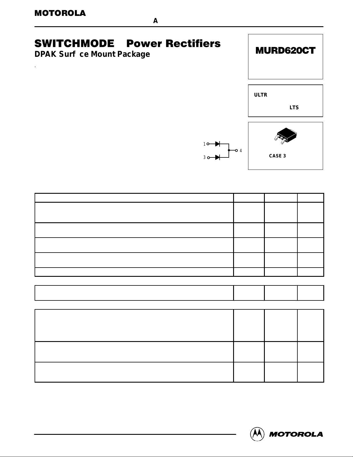
DPAK Surface Mount Package
Order this document
by MURD620CT/D
. . . designed for use in switching power supplies, inverters and as
free wheeling diodes, these state–of–the–art devices have the
following features:
• Ultrafast 35 Nanosecond Recovery Time
• Low Forward Voltage Drop
• Low Leakage
Mechanical Characteristics:
• Case: Epoxy, Molded
• Weight: 0.4 gram (approximately)
• Finish: All External Surfaces Corrosion Resistant and Terminal
Leads are Readily Solderable
• Lead and Mounting Surface Temperature for Soldering
1
Purposes: 260°C Max. for 10 Seconds
• Shipped 75 units per plastic tube
3
• Available in 16 mm Tape and Reel, 2500 units per reel, by
adding a “T4’’ suffix to the part number
• Marking: U620T
MAXIMUM RATINGS
Rating Symbol Value Unit
Peak Repetitive Reverse Voltage
Working Peak Reverse Voltage
DC Blocking Voltage
Average Rectified Forward Voltage Per Diode
(TC = 140°C, Rated VR) Per Device
Peak Repetitive Forward Current
(Rated VR, Square Wave, 20 kHz, TC = 145°C) Per Diode
Nonrepetitive Peak Surge Current
(Surge applied at rated load conditions, halfwave, 60 Hz)
Operating Junction and Storage Temperature TJ, T
THERMAL CHARACTERISTICS PER DIODE
Thermal Resistance, Junction to Case
Junction to Ambient (1)
ELECTRICAL CHARACTERISTICS PER DIODE
Maximum Instantaneous Forward Voltage Drop (2)
(iF = 3 Amps, TC = 25°C)
(iF = 3 Amps, TC = 125°C)
(iF = 6 Amps, TC = 25°C)
(iF = 6 Amps, TC = 125°C)
Maximum Instantaneous Reverse Current (2)
(TJ = 25°C, Rated dc Voltage)
(TJ = 125°C, Rated dc Voltage)
Maximum Reverse Recovery Time
(IF = 1 Amp, di/dt = 50 Amps/µs, VR = 30 V, TJ = 25°C)
(IF = 0.5 Amp, iR = 1 Amp, I
(1) Rating applies when surface mounted on the minimum pad sizes recommended.
(2) Pulse Test: Pulse Width = 300 µs, Duty Cycle ≤ 2.0%.
= 0.25 A, VR = 30 V, TJ = 25°C)
REC
MURD620CT is a
Motorola Preferred Device
ULTRAFAST RECTIFIERS
6 AMPERES
200 VOL TS
1
4
V
V
I
F(AV)
I
R
R
RRM
RWM
V
R
I
F
FSM
stg
θJC
θJA
v
F
i
R
t
rr
3
CASE 369A–13
PLASTIC
200 Volts
3
6
6 Amps
50 Amps
–65 to +175 °C
9
80
1
0.96
1.2
1.13
5
250
35
25
4
Amps
°C/W
Volts
µA
ns
SWITCHMODE is a trademark of Motorola, Inc.
Preferred devices are Motorola recommended choices for future use and best overall value.
Rev 1
Rectifier Device Data
Motorola, Inc. 1996
1

MURD620CT
100
100
70
50
30
20
10
7.0
5.0
3.0
2.0
, INSTANTANEOUS FORWARD CURRENT (AMPS)
F
i
1.0
0.7
0.5
0.3
0.2
0.1
0 0.60.2 0.8
150°C
0.4
vF, INSTANTANEOUS VOLTAGE (VOLTS)
Figure 1. T ypical Forward Voltage (Per Leg)
TJ = 25°C175°C
100°C
1.0 1.2
1.4
10
1.0
0.1
, REVERSE CURRENT (mA)
R
I
0.01
0.001
06040 100 120
20 80 200
VR, REVERSE VOLTAGE (VOLTS)
TJ = 175°C
150°C
100°C
25°C
160 180140
Figure 2. T ypical Leakage Current* (Per Leg)
* The curves shown are typical for the highest voltage device in the
voltage grouping. Typical reverse current for lower voltage selections
can be estimated from these curves if V
VR.
14
, AVERAGE POWER DISSIPATION (WA TTS)
F(AV)
P
13
12
11
10
9.0
8.0
7.0
6.0
5.0
4.0
3.0
2.0
1.0
0
IPK/IAV = 20
1.0 10
0 3.02.0
I
F(AV )
10
, AVERAGE FORW ARD CURRENT (AMPS)
is sufficiently below rated
R
SINE
5.0
WAVE
SQUARE
TJ = 175°C
6.05.04.0 9.08.07.0
Figure 3. Average Power Dissipation (Per Leg)
dc
WAVE
8.0
7.0
6.0
5.0
4.0
3.0
2.0
, AVERAGE FORW ARD CURRENT (AMPS)
1.0
F(AV)
I
2
RATED VOLTAGE APPLIED
R
q
JC
dc
SINE WAVE
OR
SQUARE WAVE
0
100
110 120 130 140 150 160 170 180
TC, CASE TEMPERATURE (°C)
Figure 4. Current Derating, Case (Per Leg)
= 9°C/W
TJ = 175°C
4.0
3.5
3.0
2.5
2.0
1.5
1.0
, AVERAGE FORW ARD CURRENT (AMPS)
0.5
0
F(AV)
I
RATED VOLTAGE APPLIED
R
= 80°C/W
q
JA
SURFACE MOUNTED ON
MIN. PAD SIZE RECOMMENDED
020
dc
SINE WAVE
OR
SQUARE WAVE
40 60 80 100
TA, AMBIENT TEMPERATURE (
120 140 160 180 200
TJ = 175°C
°
C)
Figure 5. Current Derating, Ambient (Per Leg)
Rectifier Device Data
 Loading...