

Motorola MURB1660CT Datasheet
SEMICONDUCTOR TECHNICAL DATA
Order this document
by MURB1660CT/D
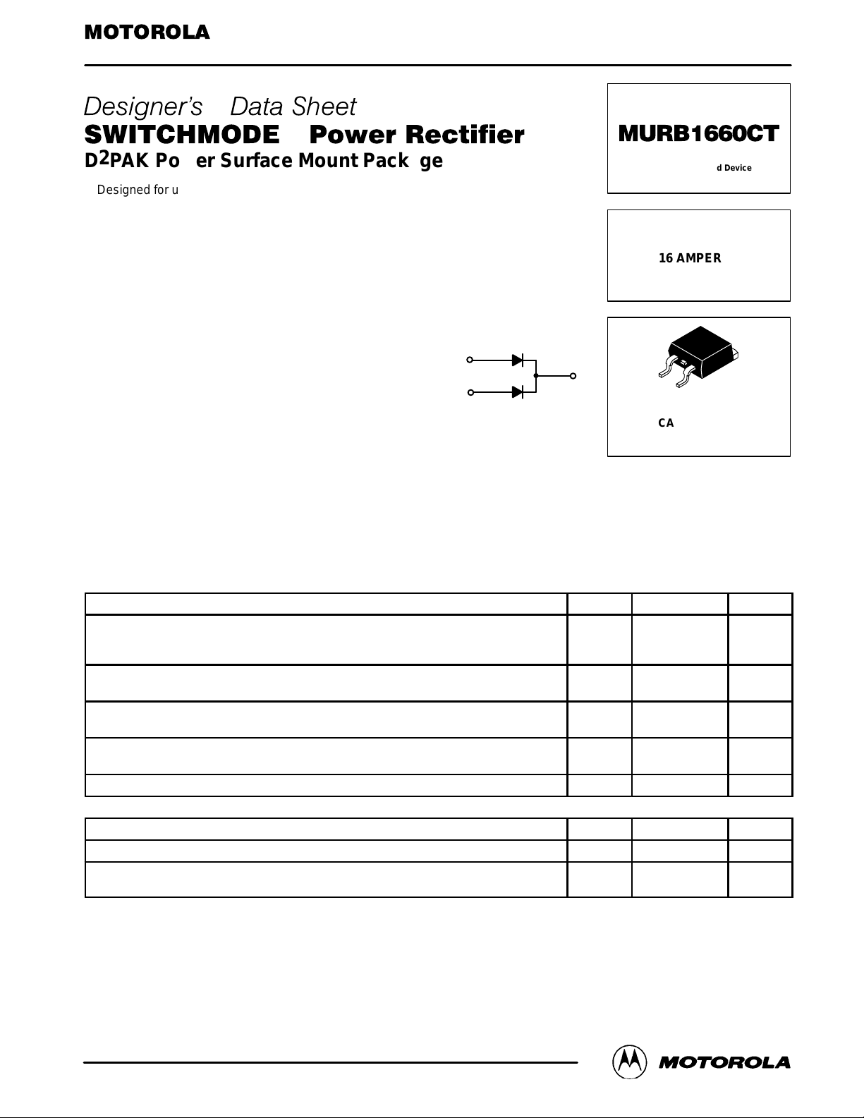
D2PAK Power Surface Mount Package
Designed for use in switching power supplies, inverters and as free wheeling
diodes, these state–of–the–art devices have the following features:
• Package Designed for Power Surface Mount Applications
• Ultrafast 60 Nanosecond Recovery Times
• 175°C Operating Junction Temperature
• Epoxy Meets UL94, VO @ 1/8″
• High Temperature Glass Passivated Junction
• High Voltage Capability to 600 V
• Low Leakage Specified @ 150°C Case Temperature
• Short Heat Sink Tab Manufactured – Not Sheared!
• Similar in Size to Industrial Standard TO–220 Package
Mechanical Characteristics
• Case: Epoxy, Molded
• Weight: 1.7 grams (approximately)
• Finish: All External Surfaces Corrosion Resistant and Terminal
Leads are Readily Solderable
• Lead and Mounting Surface Temperature for Soldering
Purposes: 260°C Max. for 10 Seconds
• Shipped 50 units per plastic tube
• Available in 24 mm Tape and Reel, 800 units per reel by
adding a “T4” suffix to the part number
• Marking: U1660T
1
3
Motorola Preferred Device
ULTRAFAST RECTIFIER
16 AMPERES
600 VOL TS
4
1
3
CASE 418B–02
D2PAK
4
MAXIMUM RATING, PER LEG
Rating Symbol Value Unit
Peak Repetitive Reverse Voltage
Working Peak Reverse Voltage
DC Blocking Voltage
Average Rectified Forward Current
Total Device, (Rated VR), TC = 150°C Total Device
Peak Repetitive Forward Current
(Rated VR, Square Wave, 20 kHz), TC = 150°C
Non–repetitive Peak Surge Current
(Surge applied at rated load conditions halfwave, single phase, 60 Hz)
Operating Junction and Storage Temperature TJ, T
V
RRM
V
RWM
V
I
F(AV)
I
FM
I
FSM
600 Volts
R
stg
8
16
16 Amps
100 Amps
– 65 to +175 °C
Amps
THERMAL CHARACTERISTICS, PER LEG
Maximum Thermal Resistance, Junction to Case R
Maximum Thermal Resistance, Junction to Ambient (1) R
Temperature for Soldering
Purposes: 1/8″ from Case for 5 Seconds
(1) See Chapter 7 for mounting conditions
Designer’s Data for “Worst Case” Conditions — The Designer’s Data Sheet permits the design of most circuits entirely from the information presented. SOA Limit
curves — representing boundaries on device characteristics — are given to facilitate “worst case” design.
Designer’s and SWITCHMODE are trademarks of Motorola, Inc.
Thermal Clad is a trademark of the Bergquist Company
Preferred devices are Motorola recommended choices for future use and best overall value.
θJC
θJA
T
L
2 °C/W
50 °C/W
260 °C
Rev 1
Rectifier Device Data
Motorola, Inc. 1996
1
MURB1660CT
ELECTRICAL CHARACTERISTICS, PER LEG
Characteristic Symbol Max Unit
Maximum Instantaneous Forward Voltage (2)
(iF = 8 Amp, TC = 150°C)
(iF = 8 Amp, TC = 25°C)
Maximum Instantaneous Reverse Current (2)
(Rated dc Voltage, TC = 150°C)
(Rated dc Voltage, TC = 25°C)
Maximum Reverse Recovery Time
(IF = 1 Amp, di/dt = 50 Amp/µs)
(IF = 0.5 Amp, iR = 1 Amp, I
(2) Pulse Test: Pulse Width = 300 µs, Duty Cycle ≤2.0%
= 0.25 Amp)
REC
v
F
i
R
t
rr
1.20
1.50
500
10
60
50
Volts
µA
ns
100
50
20
10
5.0
2.0
1.0
0.3
0.1
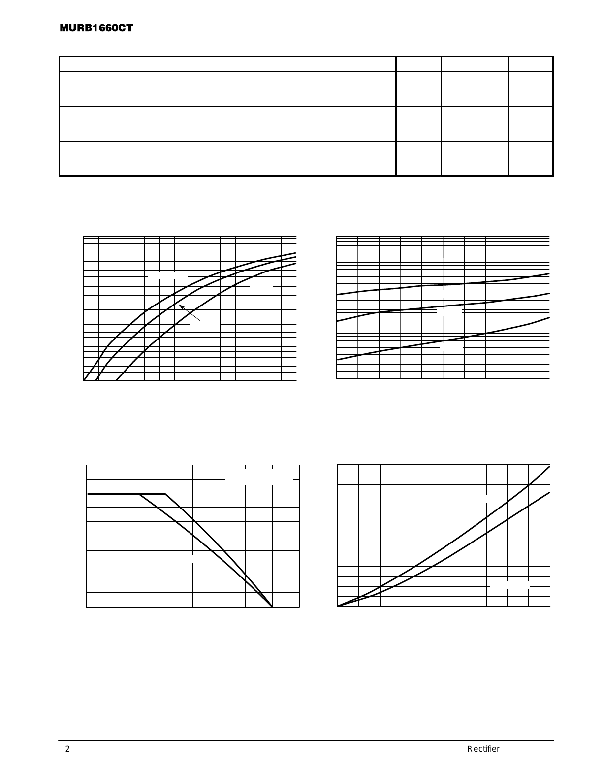
, INSTANTANEOUS FORWARD CURRENT (AMPS)
0.4 0.6 1 1.2 1.6 1.8
F
i
TJ = 150°C
25°C
100°C
0.8 1.4
vF, INSTANTANEOUS VOLTAGE (V)
Figure 1. T ypical Forward Voltage, Per Leg Figure 2. T ypical Reverse Current, Per Leg
10
9.0
8.0
7.0
6.0
5.0
4.0
3.0
2.0
, AVERAGE POWER DISSIPA TION (WATTS)
1.0
F(AV)
I
DC
SQUARE WAVE
0
TC, CASE TEMPERATURE (°C)
RATED VR APPLIED
R
= 2°C/W
θ
JC
170160150140
180
µ
, REVERSE CURRENT ( A)
R
I
10 K
1.0 K
400
100
40
10
2.0
1.0
0.4
0.1
0.04
0.01
14
13
12
11
10
9.0
8.0
7.0
6.0
5.0
4.0
3.0
, AVERAGE POWER DISSIPA TION (WATTS)
2.0
1.0
F(AV)
P
TJ = 150°C
100°C
25°C
600500400300200100
VR, REVERSE VOLTAGE (V)
SQUARE WAVE
DC
TJ = 175°C
0
I
, AVERAGE FORW ARD CURRENT (AMPS)
F(AV)
10
9876543210
Figure 3. Current Derating, Case, Per Leg Figure 4. Power Dissipation, Per Leg
2
Rectifier Device Data
 Loading...