

Motorola MUR10120E Datasheet
SEMICONDUCTOR TECHNICAL DATA
For High and Very High Resolution Monitors
Order this document
by MUR10120E/D
This state–of–the–art power rectifier is specifically designed for
use as a damper diode in horizontal deflection circuits for high and
very high resolution monitors. In these applications, the outstanding performance of the MUR10120E is fully realized when paired
with either the MJH16206 or MJF16206 monitor specific, 1200 volt
bipolar power transistor.
• 1200 Volt Blocking Voltage
• 20 mJ Avalanche Energy (Guaranteed)
• 12 Volt (Typical) Peak Transient Overshoot Voltage
• 135 ns (Typical) Forward Recovery Time
Mechanical Characteristics:
• Case: Epoxy, Molded
• Weight: 1.9 grams (approximately)
• Finish: All External Surfaces Corrosion Resistant and Terminal
Leads are Readily Solderable
• Lead Temperature for Soldering Purposes: 260°C Max. for
10 Seconds
• Shipped 50 units per plastic tube
• Marking: U10120E
MAXIMUM RATINGS
Rating Symbol Value Unit
Peak Repetitive Reverse Voltage
Working Peak Reverse Voltage
DC Blocking Voltage
Average Rectified Forward Current
(Rated VR) TC = 125°C
Peak Repetitive Forward Current, Per Leg
(Rated VR, Square Wave, 20 kHz) TC = 125°C
Nonrepetitive Peak Surge Current
(Surge applied at rated load conditions, halfwave, single phase, 60 Hz)
Operating Junction Temperature T
Controlled Avalanche Energy W
THERMAL CHARACTERISTICS
Thermal Resistance — Junction to Case R
(1) Pulse Test: Pulse Width = 300 µs, Duty Cycle ≤ 2.0%.
Motorola Preferred Device
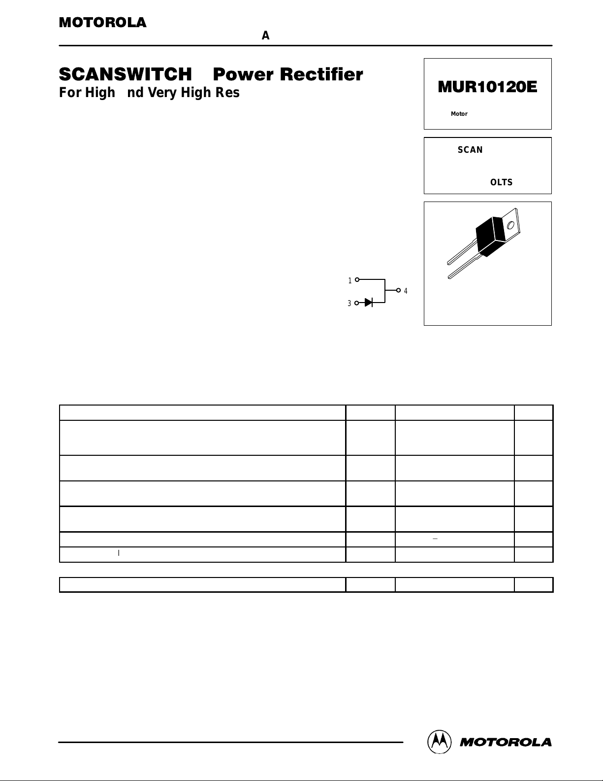
SCANSWITCH
RECTIFIER
10 AMPERES
1200 VOL TS
4
1
1
4
3
V
RRM
V
RWM
V
R
I
F(AV)
I
FRM
I
FSM
J
AVAL
θJC
3
CASE 221B–03
(TO–220AC)
STYLE 1
1200 Volts
10 Amps
20 Amps
100 Amps
*
65 to +125 °C
20 mJ
2.0 °C/W
SCANSWITCH is a trademark of Motorola, Inc.
Preferred devices are Motorola recommended choices for future use and best overall value.
Rev 1
Rectifier Device Data
Motorola, Inc. 1996
1
MUR10120E
ELECTRICAL CHARACTERISTICS
Characteristic Symbol Typ Max Unit
Maximum Instantaneous Forward Voltage (1)
(iF = 6.5 Amps, TJ = 125°C)
(iF = 6.5 Amps, TJ = 25°C)
Maximum Instantaneous Reverse Current (1)
(Rated dc Voltage, TJ = 25°C)
(Rated dc Voltage, TJ = 125°C)
Maximum Reverse Recovery Time
(IF = 1.0 A, di/dt = 50 Amps/µs)
Maximum Forward Recovery Time
IF = 6.5 Amps, di/dt = 12 Amps/µs (As Measured on a Deflection Circuit)
Peak Transient Overshoot V oltage V
(1) Pulse Test: Pulse Width = 300 µs, Duty Cycle ≤ 2.0%.
v
F
i
R
t
rr
t
fr
RFM
1.7
1.9
25
750
150 175 ns
135 175 ns
12 14 Volts
2.0
2.2
100
1000
Volts
µA
100
70
50
30
20
10
7.0
5.0
3.0
2.0
1.0
, INSTANTANEOUS FORWARD CURRENT (AMPS)
F
i
0.7
0.5
0.3
0.2
0.1
100°C
125°C
1.20.8 1.0 1.4 1.6
vF, INSTANTANEOUS VOLTAGE (VOLTS)
85°C
25°C
1000
100
m
10
1.0
, REVERSE CURRENT ( A)
R
0.1
II
0.01
200 400 600 800 1000
0
125°C
100°C
85°C
25°C
1200 1400 1600
VR, REVERSE VOLTAGE (VOLTS)
1800 2000
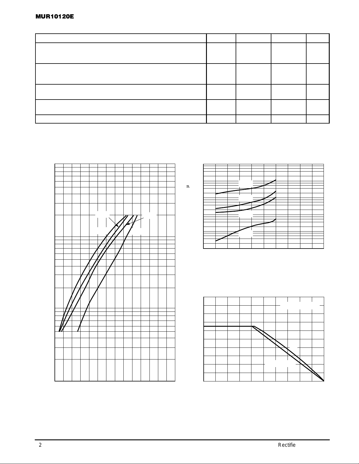
Figure 2. T ypical Reverse Current
10
9.0
8.0
7.0
6.0
5.0
4.0
3.0
2.0
, AVERAGE POWER DISSIPATION (WATTS)
1.0
0
2.0
1.80.6
F(AV)
105100
110 120
TC, CASE TEMPERATURE (
RATED VR APPLIED
dc
SQUARE WAVE
115 125
°
C)
Figure 1. T ypical Forward Voltage
2
Figure 3. Current Derating, Case
Rectifier Device Data
 Loading...