

Motorola MTY25N60E Datasheet
1
Motorola TMOS Power MOSFET Transistor Device Data
N–Channel Enhancement–Mode Silicon Gate
This advanced TMOS power FET is designed to withstand high
energy in the avalanche and commutation modes. This new energy
efficient design also o ffers a drain–to–source diode with f ast
recovery time. Designed for high voltage, high speed switching
applications in power supplies, converters, PWM motor controls,
and other inductive loads. The avalanche energy capability is
specified to eliminate the guesswork in designs where inductive
loads are switched and o ffer additional safety margin against
unexpected voltage transients.
• Avalanche Energy Specified
• Diode is Characterized for Use in Bridge Circuits
• I
DSS
and V
DS(on)
Specified at Elevated Temperature
MAXIMUM RATINGS
(TC = 25°C unless otherwise noted)
Rating
Symbol Value Unit
Drain–Source Voltage V
DSS
600 Vdc
Drain–Gate Voltage (RGS = 1 MΩ) V
DGR
600 Vdc
Gate–Source Voltage — Continuous
Gate–Source Voltage — Non–Repetitive (tp ≤ 10 ms)
V
GS
V
GSM
±20
±40
Vdc
Vpk
Drain Current — Continuous @ TC = 25°C
Drain Current — Single Pulse (tp ≤ 10 µs)
I
D
I
DM
25
65
Adc
Apk
Total Power Dissipation
Derate above 25°C
P
D
300
2.38
Watts
W/°C
Operating and Storage Temperature Range TJ, T
stg
–55 to 150 °C
Single Pulse Drain–to–Source Avalanche Energy — Starting TJ = 25°C
(VDD = 100 Vdc, VGS = 10 Vdc, Peak IL = 25 Apk, L = 10 mH, RG = 25 Ω)
E
AS
3000 mJ
Thermal Resistance — Junction to Case
Thermal Resistance — Junction to Ambient
R
θJC
R
θJA
0.42
40
°C/W
Maximum Lead Temperature for Soldering Purposes, 1/8″ from case for 10 seconds T
L
260 °C
Designer’s Data for “Worst Case” Conditions — The Designer’s Data Sheet permits the design of most circuits entirely from the information presented. SOA Limit
curves — representing boundaries on device characteristics— are given to facilitate “worst case” design.
E–FET and Designer’s are trademarks of Motorola, Inc.
TMOS is a registered trademark of Motorola, Inc.
Preferred devices are Motorola recommended choices for future use and best overall value.
REV 2
Order this document
by MTY25N60E/D
SEMICONDUCTOR TECHNICAL DATA
Motorola, Inc. 1995
TMOS POWER FET
25 AMPERES
600 VOLTS
R
DS(on)
= 0.21 OHM
CASE 340G–02, STYLE 1
TO–264
Motorola Preferred Device
D
S
G
MTY25N60E
2
Motorola TMOS Power MOSFET Transistor Device Data
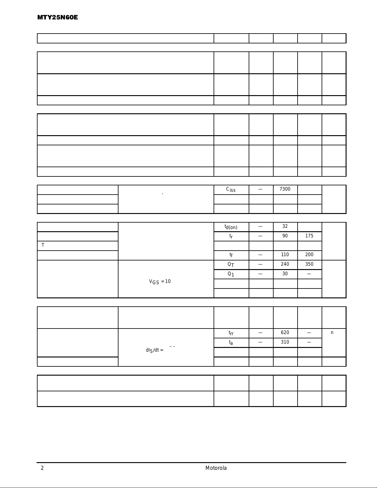
ELECTRICAL CHARACTERISTICS
(TJ = 25°C unless otherwise noted)
Characteristic
Symbol Min Typ Max Unit
OFF CHARACTERISTICS
Drain–Source Breakdown Voltage
(VGS = 0, ID = 250 µA)
Temperature Coefficient (Positive)
V
(BR)DSS
600
—
—
714
—
—
Vdc
mV/°C
Zero Gate Voltage Drain Current
(VDS = 600 Vdc, VGS = 0 Vdc)
(VDS = 600 Vdc, VGS = 0 Vdc, TJ = 125°C)
I
DSS
—
—
—
—
10
200
µAdc
Gate–Body Leakage Current (VGS = ±20 Vdc, VDS = 0) I
GSS
— — 100 nAdc
ON CHARACTERISTICS (1)
Gate Threshold Voltage
(VDS = VGS, ID = 250 µAdc)
Threshold Temperature Coefficient (Negative)
V
GS(th)
2
—
—
7
4
—
Vdc
mV/°C
Static Drain–Source On–Resistance (VGS = 10 Vdc, ID = 12.5 Adc) R
DS(on)
— — 0.21 Ohm
Drain–Source On–Voltage (VGS = 10 Vdc)
(ID = 25 Adc)
(ID = 12.5 Adc, TJ = 125°C)
V
DS(on)
—
—
5.2
—
6
7
Vdc
Forward Transconductance (VDS = 15 Vdc, ID = 12.5 Adc) g
FS
18 — — mhos
DYNAMIC CHARACTERISTICS
Input Capacitance
C
iss
— 7300 10220 pF
Output Capacitance
(VDS = 25 Vdc, VGS = 0 Vdc,
f = 1.0 MHz)
C
oss
— 700 1100
Reverse Transfer Capacitance
f = 1.0 MHz)
C
rss
— 110 250
SWITCHING CHARACTERISTICS (2)
Turn–On Delay Time
t
d(on)
— 32 60 ns
Rise Time
t
r
— 90 175
Turn–Off Delay Time
VGS = 10 Vdc,
RG = 4.7 Ω)
t
d(off)
— 170 300
Fall Time
G
= 4.7 Ω)
t
f
— 110 200
Q
T
— 240 350 nC
(See Figure 8)
DS
= 480 Vdc, ID = 25 Adc,
Q
1
— 30 —
(VDS = 480 Vdc, ID = 25 Adc,
VGS = 10 Vdc)
Q
2
— 110 —
Q
3
— 65 —
SOURCE–DRAIN DIODE CHARACTERISTICS
Forward On–Voltage
(IS = 25 Adc, VGS = 0 Vdc)
(IS = 25 Adc, VGS = 0 Vdc, TJ = 125°C)
V
SD
—
—
0.9
0.8
1.2
—
Vdc
t
rr
— 620 —
(See Figure 14)
S
= 25 Adc, VGS = 0 Vdc,
t
a
— 310 —
(IS = 25 Adc, VGS = 0 Vdc,
dIS/dt = 100 A/µs)
t
b
— 310 —
Reverse Recovery Stored Charge Q
RR
— 10.42 — µC
INTERNAL PACKAGE INDUCTANCE
Internal Drain Inductance
(Measured from the drain lead 0.25″ from package to center of die)
L
D
— 4.5 — nH
Internal Source Inductance
(Measured from the source lead 0.25″ from package to source bond pad)
L
S
— 7.5 — nH
(1) Pulse Test: Pulse Width ≤ 300 µs, Duty Cycle ≤ 2%.
(2) Switching characteristics are independent of operating junction temperature.
Gate Charge
Reverse Recovery Time
(VDD = 300 Vdc, ID = 25 Adc,
(V
(I
ns
MTY25N60E
3
Motorola TMOS Power MOSFET Transistor Device Data
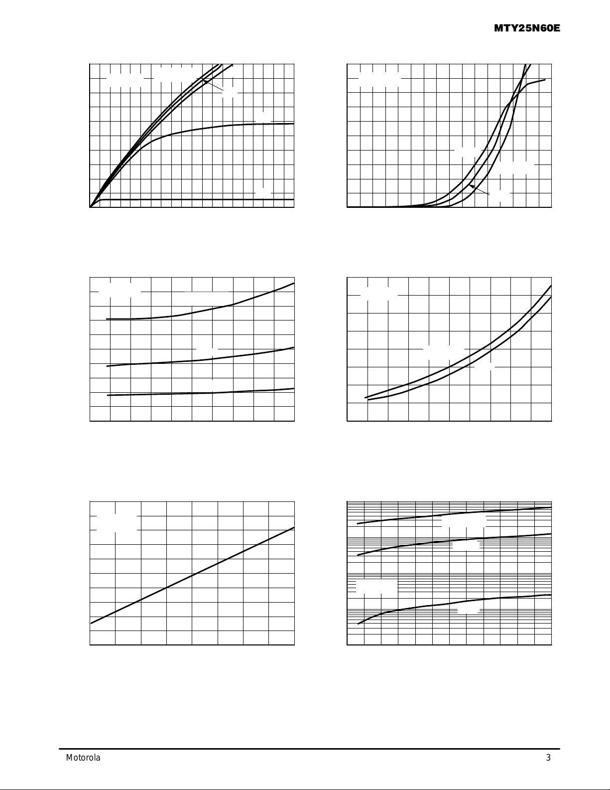
TYPICAL ELECTRICAL CHARACTERISTICS
R
DS(on)
, DRAIN–TO–SOURCE RESISTANCE
(NORMALIZED)
R
DS(on)
, DRAIN–TO–SOURCE RESISTANCE (OHMS)
R
DS(on)
, DRAIN–TO–SOURCE RESISTANCE (OHMS)
10000
1000
100
10
1
0 200 400 500 600
2.5
2
1.5
1
0.5
0
–50 –25 0 25 50 75 100 125 150
VGS = 10 V
ID = 12.5 A
0.26
0.24
0.22
0.2
0.18
ID, DRAIN CURRENT (AMPS)
15 V
0.5
0.4
0.3
0.2
0.1
0
0 20 40 50
25°C
3010
50
0
0 2 4 6 8 10 12 14 20
VDS, DRAIN–TO–SOURCE VOLTAGE (VOLTS)
Figure 1. On–Region Characteristics
I
D
, DRAIN CURRENT (AMPS)
I
D
, DRAIN CURRENT (AMPS)
VGS, GATE–TO–SOURCE VOLTAGE (VOLTS)
Figure 2. Transfer Characteristics
ID, DRAIN CURRENT (AMPS)
Figure 3. On–Resistance versus Drain Current
and Temperature
Figure 4. On–Resistance versus Drain Current
and Gate Voltage
TJ, JUNCTION TEMPERATURE (°C)
Figure 5. On–Resistance Variation with
Temperature
VDS, DRAIN–TO–SOURCE VOLTAGE (VOLTS)
Figure 6. Drain–To–Source Leakage
Current versus Voltage
I
DSS
, LEAKAGE (nA)
TJ = 25°C
VGS = 10 V
VDS ≥ 10 V
VGS = 10 V
TJ = 100°C
–55°C
TJ = 25°C
VGS = 10 V
VGS = 0 V
40
30
20
10
2 2.5 3 3.5 4 4.5 5 5.5 6
0 20 40 503010
TJ = 125°C
16 18
50
0
40
30
20
10
100 300
6 V
8 V
5 V
4 V
100°C
25°C
TJ = –55°C
25°C
100°C
 Loading...