

Motorola MTSF3N03HDR2 Datasheet
1
Motorola TMOS Power MOSFET Transistor Device Data
Medium Power Surface Mount Products
Micro8 devices are an advanced series of power MOSFETs
which utilize Motorola’s High Cell Density HDTMOS process to
achieve lowest possible on–resistance per silicon area. They are
capable of withstanding high energy in the avalanche and commuta tion modes and the drain–to–source diode has a very low reverse
recovery time. Micro8 devices are des igned for use in low voltage,
high speed switching applications where power efficiency is important.
Typical applications are dc–dc converters, and power management in
portable and battery powered products such as computers, printers,
cellular and cordless phones. They can also be used for low voltage
motor controls in mass storage products such as disk drives and tape
drives. The avalanche energy is specified to eliminate the guesswork
in designs where inductive loads are switched and offer additional
safety margin against unexpected voltage transients.
• Miniature Micro8 Surface Mount Package — Saves Board Space
• Extremely Low Profile (<1.1 mm) for thin applications such as
PCMCIA cards
• Ultra Low R
DS(on)
Provides Higher Efficiency and Extends
Battery Life
• Logic Level Gate Drive — Can Be Driven by Logic ICs
• Diode Is Characterized for Use In Bridge Circuits
• Diode Exhibits High Speed, With Soft Recovery
• I
DSS
Specified at Elevated Temperature
• Avalanche Energy Specified
• Mounting Information for Micro8 Package Provided
DEVICE MARKING ORDERING INFORMATION
Device Reel Size Tape Width Quantity
AA
MTSF3N03HDR2 13″ 12 mm embossed tape 4000 units
Designer’s Data for “Worst Case” Conditions— The Designer’s Data Sheet permits the design of most circuits entirely from the information presented. SOA Limit
curves —representing boundaries on device characteristics — are given to facilitate “worst case” design.
Preferred devices are Motorola recommended choices for future use and best overall value.
HDTMOS is a trademark of Motorola, Inc. TMOS is a registered trademark of Motorola, Inc. Micro8 is a registered trademark of International
Rectifier. Thermal Clad is a trademark of the Bergquist Company.
SEMICONDUCTOR TECHNICAL DATA
Order this document
by MTSF3N03HD/D
Motorola, Inc. 1997
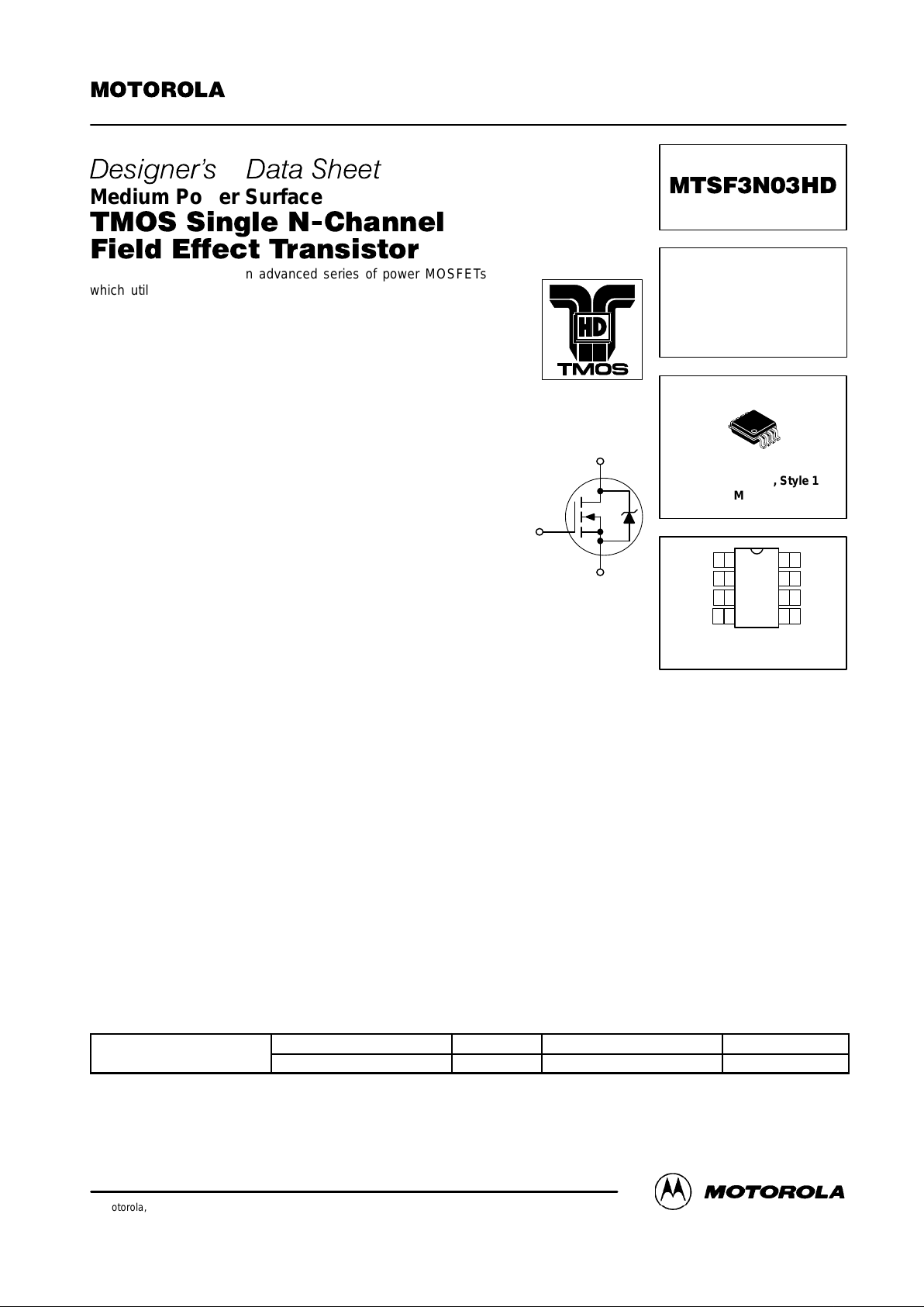
SINGLE TMOS
POWER MOSFET
3.8 AMPERES
30 VOLTS
R
DS(on)
= 0.040 OHM
CASE 846A–02, Style 1
Micro8
Motorola Preferred Device
D
S
G
Source
Source
Source
Gate
1
2
3
4
8
7
6
5
Top View
Drain
Drain
Drain
Drain
REV 3
MTSF3N03HD
2
Motorola TMOS Power MOSFET Transistor Device Data
MAXIMUM RATINGS
(TJ = 25°C unless otherwise noted)
Rating
Symbol Max Unit
Drain–to–Source Voltage V
DSS
30 V
Drain–to–Gate Voltage (RGS = 1.0 MΩ) V
DGR
30 V
Gate–to–Source Voltage — Continuous V
GS
± 20 V
1 inch SQ.
FR–4 or G–10 PCB
Figure 1 below
Steady State
Thermal Resistance — Junction to Ambient
Total Power Dissipation @ TA = 25°C
Linear Derating Factor
Drain Current — Continuous @ TA = 25°C
Continuous @ TA = 70°C
Pulsed Drain Current
(1)
R
THJA
P
D
I
D
I
D
I
DM
70
1.79
14.29
5.7
4.5
45
°C/W
Watts
mW/°C
A
A
A
Minimum
FR–4 or G–10 PCB
Figure 2 below
Steady State
Thermal Resistance — Junction to Ambient
Total Power Dissipation @ TA = 25°C
Linear Derating Factor
Drain Current — Continuous @ TA = 25°C
Continuous @ TA = 70°C
Pulsed Drain Current
(1)
R
THJA
P
D
I
D
I
D
I
DM
160
0.78
6.25
3.8
3.0
30
°C/W
Watts
mW/°C
A
A
A
Operating and Storage Temperature Range TJ, T
stg
– 55 to 150 °C
Single Pulse Drain–to–Source Avalanche Energy — Starting TJ = 25°C
(VDD = 30 Vdc, VGS = 5.0 Vdc, Peak IL = 9.0 Apk, L = 5.0 mH, RG = 25 W)
E
AS
200
mJ
(1) Repetitive rating; pulse width limited by maximum junction temperature.
Figure 1. 1.0 Inch Square FR–4 or G–10 PCB Figure 2. Minimum FR–4 or G–10 PCB
MTSF3N03HD
3
Motorola TMOS Power MOSFET Transistor Device Data
ELECTRICAL CHARACTERISTICS (T
A
= 25°C unless otherwise noted)
Characteristic Symbol Min Typ Max Unit
OFF CHARACTERISTICS
Drain–to–Source Breakdown Voltage (Cpk ≥ 2.0) (1) (3)
(VGS = 0 Vdc, ID = 250 µAdc)
T emperature Coef ficient (Positive)
V
(BR)DSS
30
—
—
27
—
—
Vdc
mV/°C
Zero Gate Voltage Drain Current
(VDS = 24 Vdc, VGS = 0 Vdc)
(VDS = 24 Vdc, VGS = 0 Vdc, TJ = 125°C)
I
DSS
—
—
—
—
1.0
25
µAdc
Gate–Body Leakage Current (VGS = ± 20 Vdc, VDS = 0) I
GSS
— — 100 nAdc
ON CHARACTERISTICS
(1)
Gate Threshold Voltage (Cpk ≥ 2.0) (3)
(VDS = VGS, ID = 250 µAdc)
Threshold Temperature Coefficient (Negative)
V
GS(th)
1.0
—
1.5
4.5
—
—
Vdc
mV/°C
Static Drain–to–Source On–Resistance (Cpk ≥ 2.0) (3)
(VGS = 10 Vdc, ID = 3.8 Adc)
(VGS = 4.5 Vdc, ID = 1.9 Adc)
R
DS(on)
—
—
35
45
40
60
mΩ
Forward Transconductance (VDS = 10 Vdc, ID = 1.9 Adc) g
FS
2.0 — — Mhos
DYNAMIC CHARACTERISTICS
Input Capacitance
C
iss
— 420 — pF
Output Capacitance
(VDS = 25 Vdc, VGS = 0 Vdc,
f = 1.0 MHz
)
C
oss
— 190 —
Transfer Capacitance
f = 1.0 MHz)
C
rss
— 65 —
SWITCHING CHARACTERISTICS
(2)
Turn–On Delay Time
t
d(on)
— 7.0 — ns
Rise Time
(VDS = 15 Vdc, ID = 3.7 Adc,
t
r
— 19 —
Turn–Off Delay Time
(
DS
,
D
,
VGS = 10 Vdc, RG = 6 Ω) (1)
t
d(off)
— 32 —
Fall Time t
f
— 36 —
Turn–On Delay Time
t
d(on)
— 7.0 — ns
Rise Time
(VDD = 15 Vdc, ID = 1.9 Adc,
t
r
— 11 —
Turn–Off Delay Time
(
DD
,
D
,
VGS = 4.5 Vdc, RG = 6 Ω) (1)
t
d(off)
— 29 —
Fall Time t
f
— 23 —
Gate Charge
Q
T
— 18.5 26 nC
(VDS = 24 Vdc, ID = 3.7 Adc,
Q
1
— 1.4 —
(
DS
,
D
,
VGS = 10 Vdc)
Q
2
— 5.5 —
Q
3
— 7.1 —
SOURCE–DRAIN DIODE CHARACTERISTICS
Forward On–Voltage
(IS = 3.7 Adc, VGS = 0 Vdc) (1)
(IS = 3.7 Adc, VGS = 0 Vdc, TJ = 125°C)
V
SD
—
—
0.82
0.7
1.0
—
Vdc
Reverse Recovery Time
t
rr
— 28 —
ns
(IS = 3.7 Adc, VGS = 0 Vdc,
dI
/dt = 100 A/µs) (1
)
t
a
— 14 —
dIS/dt = 100 A/µs)
(1)
t
b
— 14 —
Reverse Recovery Storage Charge Q
RR
— 0.028 — µC
(1) Pulse Test: Pulse Width ≤ 300 µs, Duty Cycle ≤ 2%.
(2) Switching characteristics are independent of operating junction temperature.
(3) Reflects typical values.
Cpk =
Max limit – Typ
3 x SIGMA
MTSF3N03HD
4
Motorola TMOS Power MOSFET Transistor Device Data
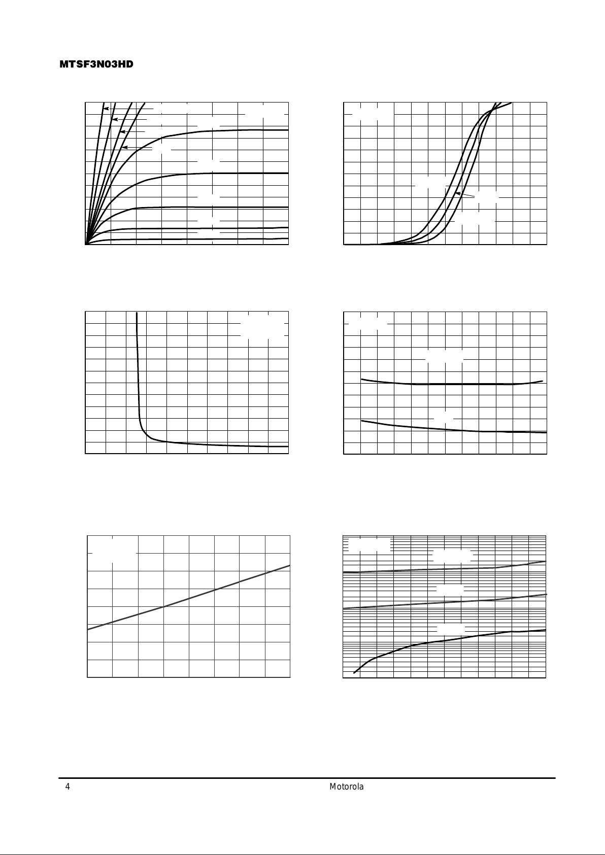
TYPICAL ELECTRICAL CHARACTERISTICS
I
DSS
, LEAKAGE (nA)
R
DS(on)
, DRAIN–TO–SOURCE RESIST ANCE (OHMS)
R
DS(on)
, DRAIN–TO–SOURCE RESIST ANCE (OHMS)
0
0 0.5 1.5 2
0
1
3
VDS, DRAIN–TO–SOURCE VOL TAGE (VOLTS)
Figure 3. On–Region Characteristics
I
D
, DRAIN CURRENT (AMPS)
I
D
, DRAIN CURRENT (AMPS)
VGS, GATE–T O–SOURCE VOLTAGE (VOLTS)
Figure 4. Transfer Characteristics
0.4
0.5
0.6
0.03
Figure 5. On–Resistance versus
Gate–to–Source Voltage
ID, DRAIN CURRENT (AMPS)
Figure 6. On–Resistance versus Drain Current
and Gate Voltage
1
100
Figure 7. On–Resistance Variation
with Temperature
VDS, DRAIN–TO–SOURCE VOL TAGE (VOLTS)
Figure 8. Drain–to–Source Leakage Current
versus Voltage
VDS ≥ 10 V
TJ = –55°C
25°C
100°C
0.3
4
2
0.1
TJ = 25°C
2
4
6
5
1
2 2.5 3 3.5 4
0.2
0.06
012 56
10
0 5 10 15 30
2.3 V
20 25
0
0.04
0.05
3
24 86
10
VGS, GATE–T O–SOURCE VOLT AGE (VOLTS)
34
10 V
VGS = 4.5
TJ = 25°C
R
DS(on)
, DRAIN–TO–SOURCE RESIST ANCE (NORMALIZED)
TJ, JUNCTION TEMPERATURE (°C)
–50 0 50 100 150
0
0.5
1.0
1.5
2.0
VGS = 10 V
ID = 1.9 A
1257525–25
VGS = 0 V
TJ = 125°C
100°C
1
5
6
2.1 V
2.5 V
2.7 V
2.9 V
3.1 V
4.5 V
VGS = 10 V
ID = 3.8 A
TJ = 25
°
C
3.3 V
1.51
0
0.035
0.045
0.055
1000
0.1
25°C
 Loading...