

Motorola MTP40N10E Datasheet

SEMICONDUCTOR TECHNICAL DATA
Order this document
by MTP40N10E/D
N–Channel Enhancement–Mode Silicon Gate
This advanced TMOS E–FET is designed to withstand high
energy in the avalanche and commutation modes. The new energy
efficient design also offers a drain–to–source diode with a fast
recovery time. Designed for low voltage, high speed switching
applications in power supplies, converters and PWM motor
controls, these devices are particularly well suited for bridge circuits
where diode speed and commutating safe operating areas are
critical and offer additional safety margin against unexpected
voltage transients.
• Avalanche Energy Specified
• Source–to–Drain Diode Recovery Time Comparable to a
Discrete Fast Recovery Diode
• Diode is Characterized for Use in Bridge Circuits
• I
DSS
and V
Specified at Elevated Temperature
DS(on)
G
N–Channel
D
S
TMOS POWER FET
40 AMPERES
100 VOL TS
R
CASE 221A–06, Style 5
DS(on)
TO–220AB
= 0.04 OHM
MAXIMUM RATINGS
Drain–to–Source Voltage V
Drain–to–Gate Voltage (RGS = 1.0 MΩ) V
Gate–to–Source Voltage — Continuous
Gate–to–Source Voltage — Non–Repetitive (tp ≤ 10 ms)
Drain Current — Continuous
Drain Current — Continuous @ 100°C
Drain Current — Single Pulse (tp ≤ 10 µs)
Total Power Dissipation
Derate above 25°C
Operating and Storage Temperature Range TJ, T
Single Pulse Drain–to–Source Avalanche Energy — Starting TJ = 25°C
(VDD = 75 Vdc, VGS = 10 Vdc, PEAK IL = 40 Apk, L = 1.0 mH, RG = 25 W)
Thermal Resistance — Junction to Case
Thermal Resistance — Junction to Ambient
Maximum Lead Temperature for Soldering Purposes, 1/8″ from case for 10 seconds T
This document contains information on a new product. Specifications and information herein are subject to change without notice.
E–FET is a trademark of Motorola, Inc. TMOS is a registered trademark of Motorola, Inc.
(TC = 25°C unless otherwise noted)
Rating
Symbol Value Unit
DSS
DGR
V
GS
V
GSM
I
D
I
D
I
DM
P
D
stg
E
AS
R
θJC
R
θJA
L
100 Vdc
100 Vdc
±20
±40
40
29
140
169
1.35
–55 to 150 °C
800 mJ
0.74
62.5
260 °C
Vdc
Vpk
Adc
Apk
Watts
W/°C
°C/W
REV 1
Motorola TMOS Power MOSFET Transistor Device Data
Motorola, Inc. 1997
1
MTP40N10E
)
f = 1.0 MHz)
V
G
)
(
DS
,
D
,
(
S
,
GS
,
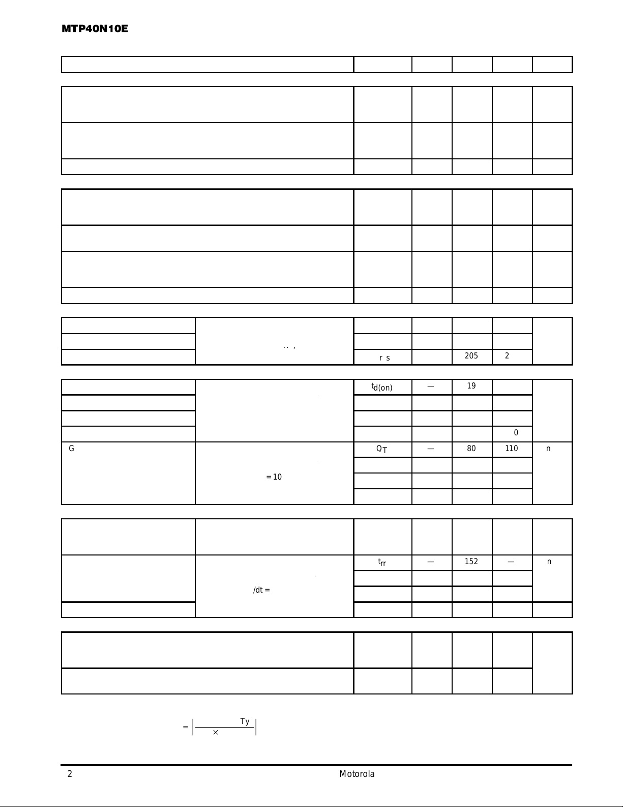
ELECTRICAL CHARACTERISTICS
OFF CHARACTERISTICS
Drain–to–Source Breakdown Voltage
(VGS = 0 Vdc, ID = 0.25 mAdc)
T emperature Coef ficient (Positive) (Cpk ≥ 2.0)
Zero Gate Voltage Drain Current
(VDS = 100 Vdc, VGS = 0 Vdc)
(VDS = 100 Vdc, VGS = 0 Vdc, TJ =125°C)
Gate–Body Leakage Current (VGS = ±20 Vdc, VDS = 0 Vdc) I
ON CHARACTERISTICS
Gate Threshold Voltage (Cpk ≥ 2.0)
(VDS = VGS, ID = 250 µAdc)
Threshold Temperature Coefficient (Negative)
Static Drain–to–Source On–Resistance (Cpk ≥ 2.0)
(VGS = 10 Vdc, ID = 20 Adc)
Drain–to–Source On–Voltage
(VGS = 10 Vdc, ID = 40 Adc)
(VGS = 10 Vdc, ID = 20 Adc, TJ = 125°C)
Forward Transconductance (VDS = 8.4 Vdc, ID = 20 Adc) g
DYNAMIC CHARACTERISTICS
Input Capacitance
Output Capacitance
Transfer Capacitance
SWITCHING CHARACTERISTICS
Turn–On Delay Time
Rise Time
Turn–Off Delay Time
Fall Time
Gate Charge
(See Figure 8)
SOURCE–DRAIN DIODE CHARACTERISTICS
Forward On–Voltage
Reverse Recovery Time
(See Figure 14)
Reverse Recovery Stored Charge Q
INTERNAL PACKAGE INDUCTANCE
Internal Drain Inductance
(Measured from contact screw on tab to center of die)
(Measured from the drain lead 0.25″ from package to center of die)
Internal Source Inductance
(Measured from the source lead 0.25″ from package to source bond pad)
(1) Pulse Test: Pulse Width ≤ 300 µs, Duty Cycle ≤ 2%.
(2) Switching characteristics are independent of operating junction temperature.
(3) Reflects typical values.
(1)
Cpk
(T
= 25°C unless otherwise noted)
J
Characteristic
(VDS = 25 Vdc, VGS = 0 Vdc,
(2)
(IS = 40 Adc, VGS = 0 Vdc, TJ = 125°C)
Max limit – Typ
Ť
+
3 sigma
f = 1.0 MHz
(VDD = 50 Vdc, ID = 40 Adc,
(VDS = 80 Vdc, ID = 40 Adc,
(IS = 40 Adc, VGS = 0 Vdc)
(IS = 40 Adc, VGS = 0 Vdc,
= 10 Vdc,
GS
RG = 9.1 Ω)
VGS = 10 Vdc)
dIS/dt = 100 A/µs)
Ť
(3)
(3)
(3)
Symbol Min Typ Max Unit
V
(BR)DSS
I
DSS
GSS
V
GS(th)
R
DS(on)
V
DS(on)
FS
C
iss
C
oss
C
rss
t
d(on)
t
r
t
d(off)
t
f
Q
T
Q
1
Q
2
Q
3
V
SD
t
rr
t
a
t
b
RR
L
D
L
S
100
—
—
—
— — 100 nAdc
2.0
—
— 0.033 0.04
—
—
17 21 — mhos
— 2305 3230 pF
— 620 1240
— 205 290
— 19 40 ns
— 165 330
— 75 150
— 97 190
— 80 110 nC
— 15 —
— 40 —
— 29 —
—
—
— 152 —
— 117 —
— 35 —
— 1.0 — µC
—
—
— 7.5 —
—
112
—
—
2.9
6.7
—
—
0.96
0.88
3.5
4.5
—
—
10
100
4.0
—
1.9
1.7
1.0
—
—
—
mV/°C
mV/°C
Ohms
Vdc
µAdc
Vdc
Vdc
Vdc
ns
nH
2
Motorola TMOS Power MOSFET Transistor Device Data

TYPICAL ELECTRICAL CHARACTERISTICS
MTP40N10E
80
VGS = 10 V TJ = 25°C
70
60
50
40
30
, DRAIN CURRENT (AMPS)
20
D
I
10
0
012345678910
VDS, DRAIN–TO–SOURCE VOL TAGE (VOLTS)
8 V
9 V
Figure 1. On–Region Characteristics
0.07
VGS = 10 V
0.06
0.05
0.04
0.03
0.02
, DRAIN–TO–SOURCE RESIST ANCE (OHMS)
0.01
0
DS(on)
R
01020304050607080
TJ = 100°C
25°C
–55°C
ID, DRAIN CURRENT (AMPS)
7 V
6 V
5 V
80
VDS ≥ 10 V
70
60
50
40
30
, DRAIN CURRENT (AMPS)
20
D
I
10
0
23 4 5 67 8
VGS, GATE–T O–SOURCE VOLTAGE (VOLTS)
100°C
25°C
TJ = –55°C
Figure 2. Transfer Characteristics
0.050
TJ = 25°C
0.045
0.040
0.035
0.030
0.025
0.020
, DRAIN–TO–SOURCE RESIST ANCE (OHMS)
0.015
0.010
DS(on)
R
01020304050607080
VGS = 10 V
15 V
ID, DRAIN CURRENT (AMPS)
Figure 3. On–Resistance versus Drain Current
and T emperature
2.0
1.8
VGS = 10 V
ID = 20 A
1.6
1.4
1.2
1.0
0.8
(NORMALIZED)
0.6
, DRAIN–TO–SOURCE RESIST ANCE
0.4
0.2
DS(on)
R
0
–50 –25 0 25 50 75 100 125 150
TJ, JUNCTION TEMPERATURE (°C)
Figure 5. On–Resistance Variation with
Temperature
Figure 4. On–Resistance versus Drain Current
and Gate Voltage
1000
, LEAKAGE (nA)
DSS
I
VGS = 0 V
100
10
1.0
010203040 607080 100
VDS, DRAIN–TO–SOURCE VOL TAGE (VOLTS)
TJ = 125°C
100°C
50 90
Figure 6. Drain–T o–Source Leakage
Current versus Voltage
Motorola TMOS Power MOSFET Transistor Device Data
3
 Loading...