

Motorola MTP3N50E Datasheet
1
Motorola TMOS Power MOSFET Transistor Device Data
N–Channel Enhancement–Mode Silicon Gate
This a dvanced h igh voltage TMOS E–FET is designed to
withstand high energy in the avalanche mode and switch efficiently.
This new high energy device also offers a drain–to–source diode
with fast recovery time. Designed for high voltage, high s peed
switching applications such a s power supplies, P WM motor
controls and other inductive loads, the avalanche energy capability
is specified to eliminate the guesswork in designs where inductive
loads are switched and offer additional s afety margin against
unexpected voltage transients.
• Avalanche Energy Capability Specified at Elevated
Temperature
• Low Stored Gate Charge for Efficient Switching
• Internal Source–to–Drain Diode Designed to Replace External
Zener Transient Suppressor — Absorbs High Energy in the
Avalanche Mode
• Source–to–Drain Diode Recovery Time Comparable to Discrete
Fast Recovery Diode
MAXIMUM RATINGS
(TC = 25°C unless otherwise noted)
Rating
Symbol Value Unit
Drain–Source Voltage V
DSS
500 Vdc
Drain–Gate Voltage (RGS = 1.0 MΩ) V
DGR
500 Vdc
Gate–Source Voltage — Continuous
Gate–Source Voltage — Non–repetitive (tp ≤ 50 µs)
V
GS
V
GSM
±20
±40
Vdc
Vpk
Drain Current — Continuous
Drain Current — Pulsed
I
D
I
DM
3.0
10
Adc
Total Power Dissipation @ TC = 25°C
Derate above 25°C
P
D
50
0.4
Watts
W/°C
Operating and Storage Temperature Range TJ, T
stg
–65 to 150 °C
UNCLAMPED DRAIN–TO–SOURCE AVALANCHE CHARACTERISTICS (T
J
< 150°C)
Single Pulse Drain–to–Source Avalanche Energy — TJ = 25°C
Single Pulse Drain–to–Source Avalanche Energy — TJ = 100°C
Repetitive Pulse Drain–to–Source Avalanche Energy
W
DSR
(1)
W
DSR
(2)
210
33
5.0
mJ
THERMAL CHARACTERISTICS
Thermal Resistance — Junction to Case°
— Junction to Ambient°
R
θJC
R
θJA
2.5
62.5
°C/W
Maximum Lead Temperature for Soldering Purposes, 1/8″ from case for 10 seconds T
L
260 °C
(1) VDD = 50 V, ID = 3.0 A
(2) Pulse Width and frequency is limited by TJ(max) and thermal response
Designer’s Data for “Worst Case” Conditions — The Designer’s Data Sheet permits the design of most circuits entirely from the information presented. SOA Limit
curves — representing boundaries on device characteristics— are given to facilitate “worst case” design.
E–FET and Designer’s are trademarks of Motorola, Inc. TMOS is a registered trademark of Motorola, Inc.
Preferred devices are Motorola recommended choices for future use and best overall value.
REV 1
Order this document
by MTP3N50E/D
SEMICONDUCTOR TECHNICAL DATA
TMOS POWER FET
3.0 AMPERES
500 VOLTS
R
DS(on)
= 3.0 OHMS
D
S
G
CASE 221A–06, Style 5
TO–220AB
Motorola Preferred Device
Motorola, Inc. 1996
MTP3N50E
2
Motorola TMOS Power MOSFET Transistor Device Data
ELECTRICAL CHARACTERISTICS
(T
J
= 25°C unless otherwise noted)
Characteristic
Symbol Min Typ Max Unit
OFF CHARACTERISTICS
Drain–to–Source Breakdown Voltage
(VGS = 0, ID = 0.25 mA)
V
(BR)DSS
500 — — Vdc
Zero Gate Voltage Drain Current
(VDS = 500 V, VGS = 0)
(VDS = 400 V, VGS = 0, TJ = 125°C)
I
DSS
—
—
—
—
0.25
1.0
mAdc
Gate–Body Leakage Current, Forward (V
GSF
= 20 Vdc, VDS = 0) I
GSSF
— — 100 nAdc
Gate–Body Leakage Current, Reverse (V
GSR
= 20 Vdc, VDS = 0) I
GSSR
— — 100 nAdc
ON CHARACTERISTICS*
Gate Threshold Voltage
(VDS = VGS, ID = 0.25 mAdc)
(TJ = 125°C)
V
GS(th)
2.0
1.5
—
—
4.0
3.5
Vdc
Static Drain–Source On–Resistance (VGS = 10 Vdc, ID = 1.5 Adc) R
DS(on)
— 2.4 3.0 Ohm
Drain–Source On–Voltage (VGS = 10 Vdc)
(ID = 3.0 A)
(ID = 1.5 A, TJ = 100°C)
V
DS(on)
—
—
—
—
10
8.0
Vdc
Forward Transconductance (VDS = 15 Vdc, ID = 1.5 Adc) g
FS
1.0 — — mhos
DYNAMIC CHARACTERISTICS
Input Capacitance
C
iss
— 435 — pF
Output Capacitance
(VDS = 25 V, VGS = 0,
f = 1.0 MHz)
C
oss
— 56 —
Transfer Capacitance
f = 1.0 MHz)
C
rss
— 9.2 —
SWITCHING CHARACTERISTICS*
Turn–On Delay Time
t
d(on)
— 14 — ns
Rise Time
≈ 3.0 A,
t
r
— 14 —
Turn–Off Delay Time
RG = 18 Ω, RL = 83 Ω,
V
GS(on)
= 10 V)
t
d(off)
— 30 —
Fall Time
GS(on)
= 10 V)
t
f
— 20 —
Total Gate Charge
Q
g
— 15 21 nC
Gate–Source Charge
(VDS = 400 V, ID = 3.0 A,
V
= 10 V)
Q
gs
— 2.5 —
Gate–Drain Charge
VGS = 10 V)
Q
gd
— 10 —
SOURCE–DRAIN DIODE CHARACTERISTICS*
Forward On–Voltage (IS = 3.0 A) V
SD
— — 1.5 Vdc
Forward Turn–On Time
t
on
— ** —
Reverse Recovery Time
(IS = 3.0 A, di/dt = 100 A/µs)
t
rr
— 200 —
INTERNAL PACKAGE INDUCTANCE
Internal Drain Inductance
(Measured from the contact screw on tab to center of die)
(Measured from the drain lead 0.25″ from package to center of die)
L
d
—
—
3.5
4.5
—
—
Internal Source Inductance
(Measured from the source lead 0.25″ from package to source bond pad)
L
s
— 7.5 —
*Indicates Pulse Test: Pulse Width = 300 µs Max, Duty Cycle ≤ 2.0%.
**Limited by circuit inductance.
(VDD = 250 V, ID
ns
nH
MTP3N50E
3
Motorola TMOS Power MOSFET Transistor Device Data
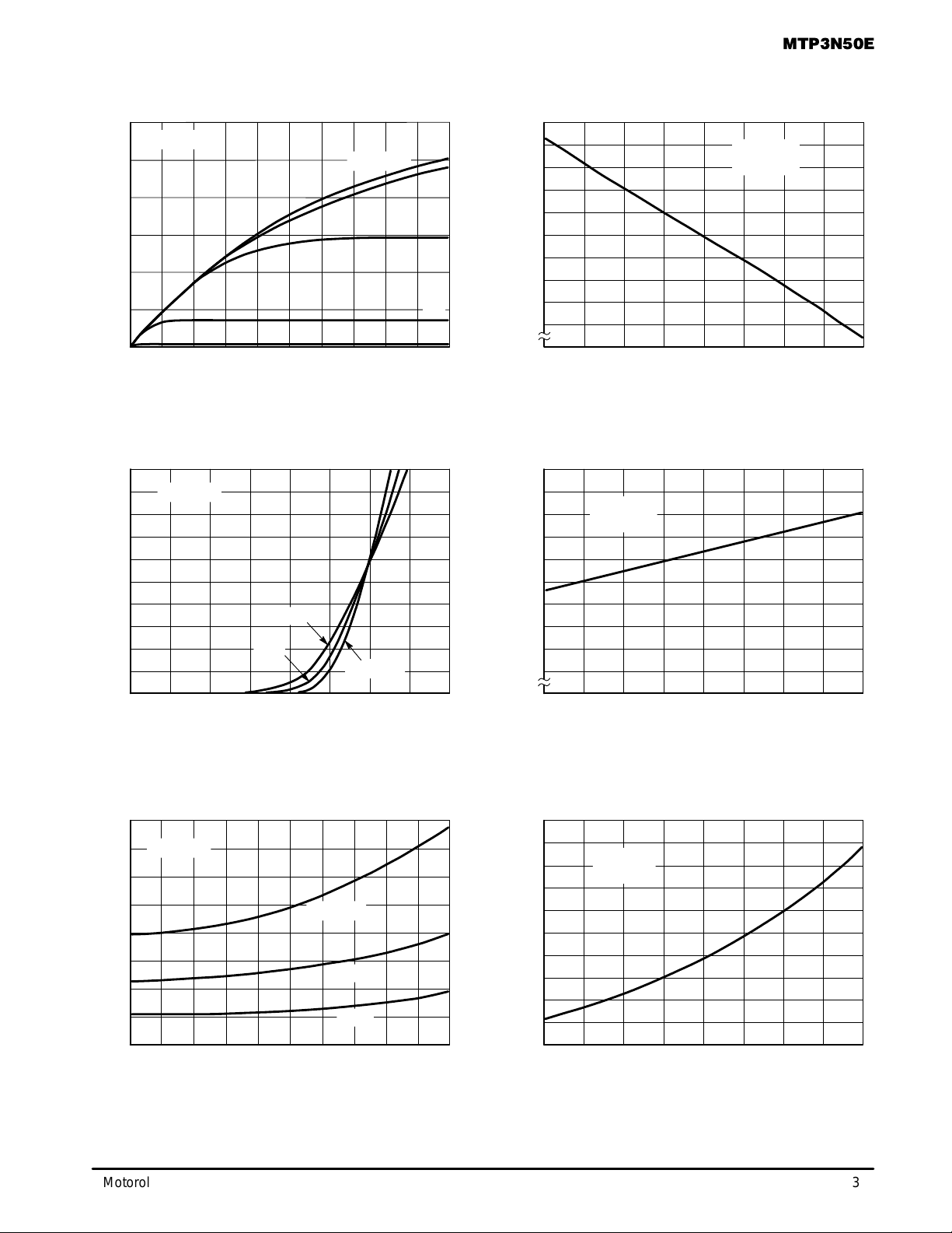
TYPICAL ELECTRICAL CHARACTERISTICS
VDS, DRAIN–TO–SOURCE VOLTAGE (VOLTS)
Figure 1. On–Region Characteristics
TJ, JUNCTION TEMPERATURE (°C)
Figure 2. Gate–Threshold Voltage Variation
With Temperature
VGS, GATE–TO–SOURCE VOLTAGE (VOLTS)
Figure 3. Transfer Characteristics
TJ, JUNCTION TEMPERATURE (°C)
Figure 4. Breakdown Voltage Variation
With Temperature
ID, DRAIN CURRENT (AMPS)
Figure 5. On–Resistance versus Drain Current
TJ, JUNCTION TEMPERATURE (°C)
Figure 6. On–Resistance versus Temperature
R
DS(on)
, DRAIN–TO–SOURCE RESISTANCE (OHMS)
R
DS(on)
, DRAIN–TO–SOURCE RESISTANCE
(NORMALIZED)
I
D
, DRAIN CURRENT (AMPS)
V
GS(th)
, GATE THRESHOLD VOLTAGE (NORMALIZED)
V
BR(DSS)
, DRAIN–TO–SOURCE BREAKDOWN VOLTAGE
(NORMALIZED)
6
5
4
3
2
201612840
1.2
1.1
1
0.9
0.8
–50 –25 0 25 50 75 100 125 150
5
4
3
2
1
0
86420
1.2
1.1
1
0.9
0.8
–50 0 50 100 150
8
6
4
2
543210
2.5
2
1.5
1
0.5
TJ = 25°C
7 V
6 V
5 V
VDS = V
GS
ID = 0.25 mA
TJ = –55°C
25°C
100°C
VGS = 0
ID = 250
µ
A
TJ = 100°C
25°C
–55°C
VGS = 10 V
VGS = 10 V
ID = 1.5 A
I
D
, DRAIN CURRENT (AMPS)
VGS = 10 V
4 V
VDS ≥ 10 V
1
0
2 6 10 14 18
0
–50 –25 0 25 50 75 100 125 150
 Loading...