

Motorola MTP3N120E Datasheet
1
Motorola TMOS Power MOSFET Transistor Device Data
N–Channel Enhancement–Mode Silicon Gate
This advanced high–voltage T MOS E–FET is d esigned to
withstand high energy in the avalanche mode and switch efficiently.
This new high energy device also offers a drain–to–source diode
with fast recovery time. Designed for high voltage, high speed
switching applications such as power supplies, PWM m otor
controls, and other inductive loads, the avalanche energy capability
is specified to eliminate the guesswork in designs where inductive
loads are switched a nd offer additional s afety margin against
unexpected voltage transients.
• Avalanche Energy Capability Specified at Elevated
Temperature
• Low Stored Gate Charge for Efficient Switching
• Internal Source–to–Drain Diode Designed to Replace External
Zener Transient Suppressor Absorbs High Energy in the
Avalanche Mode
• Source–to–Drain Diode Recovery Time Comparable to
Discrete Fast Recovery Diode
* See App. Note AN1327 — Very Wide Input Voltage Range;
Off–line Flyback Switching Power Supply
MAXIMUM RATINGS
(TC = 25°C unless otherwise noted)
Rating
Symbol Value Unit
Drain–Source Voltage V
DSS
1200 Vdc
Drain–Gate Voltage (RGS = 1.0 MΩ) V
DGR
1200 Vdc
Gate–Source Voltage — Continuous
Gate–Source Voltage — Non–Repetitive (tp ≤ 50 ms)
V
GS
V
GSM
± 20
± 40
Vdc
Vpk
Drain Current — Continuous @ 25°C
Drain Current — Continuous @ 100°C
Drain Current — Single Pulse (tp ≤ 10 µs)
I
D
I
D
I
DM
3.0
2.2
11
Adc
Apk
Total Power Dissipation
Derate above 25°C
P
D
125
1.0
Watts
W/°C
Operating and Storage Temperature Range TJ, T
stg
– 55 to 150 °C
UNCLAMPED DRAIN–TO–SOURCE AVALANCHE CHARACTERISTICS (T
J
t150°C)
Single Pulse Drain–to–Source Avalanche Energy — Starting TJ = 25°C
(VDD = 100 Vdc, VGS = 10 Vdc, PEAK IL = 4.5 Apk, L = 10 mH, RG = 25 Ω)
E
AS
101
mJ
THERMAL CHARACTERISTICS
Thermal Resistance — Junction to Case
Thermal Resistance — Junction to Ambient
R
θJC
R
θJA
1.0
62.5
°C/W
Maximum Lead Temperature for Soldering Purposes, 1/8″ from case for 10 seconds T
L
260 °C
E–FET and Designer’s are trademarks of Motorola, Inc.
TMOS is a registered trademark of Motorola, Inc.
Preferred devices are Motorola recommended choices for future use and best overall value.
REV 1
SEMICONDUCTOR TECHNICAL DATA
Order this document
by MTP3N120E/D
Motorola, Inc. 1995
TMOS POWER FET
3.0 AMPERES
1200 VOLTS
R
DS(on)
= 5.0 OHM
Motorola Preferred Device
D
S
G
CASE 221A–06, Style 5
TO–220AB
MTP3N120E
2
Motorola TMOS Power MOSFET Transistor Device Data
ELECTRICAL CHARACTERISTICS
(T
J
= 25°C unless otherwise noted)
Characteristic
Symbol Min Typ Max Unit
OFF CHARACTERISTICS
Drain–Source Breakdown Voltage
(VGS = 0 Vdc, ID = 250 µAdc)
Temperature Coefficient (Positive)
V
(BR)DSS
1200
—
—
1.28
—
—
Vdc
mV/°C
Zero Gate Voltage Drain Current
(VDS = 1200 Vdc, VGS = 0 Vdc)
(VDS = 1200 Vdc, VGS = 0 Vdc, TJ = 125°C)
I
DSS
—
—
—
—
10
100
µAdc
Gate–Body Leakage Current (VGS = ± 20 Vdc, VDS = 0 Vdc) I
GSS
— — 100 nAdc
ON CHARACTERISTICS (1)
Gate Threshold Voltage
(VDS = VGS, ID = 250 µAdc)
Temperature Coefficient (Negative)
V
GS(th)
2.0
—
3.0
7.1
4.0
—
Vdc
mV/°C
Static Drain–Source On–Resistance (VGS = 10 Vdc, ID = 1.5 Adc) R
DS(on)
— 4.0 5.0 Ohm
Drain–Source On–Voltage (VGS = 10 Vdc)
(ID = 3.0 Adc)
(ID = 1.5 Adc, TJ = 125°C)
V
DS(on)
—
—
—
—
18.0
15.8
Vdc
Forward Transconductance (VDS = 15 Vdc, ID = 1.5 Adc) g
FS
2.5 3.1 — mhos
DYNAMIC CHARACTERISTICS
Input Capacitance
C
iss
— 2130 2980 pF
Output Capacitance
(VDS = 25 Vdc, VGS = 0 Vdc,
f = 1.0 MHz)
C
oss
— 1710 2390
Reverse Transfer Capacitance
f = 1.0 MHz)
C
rss
— 932 1860
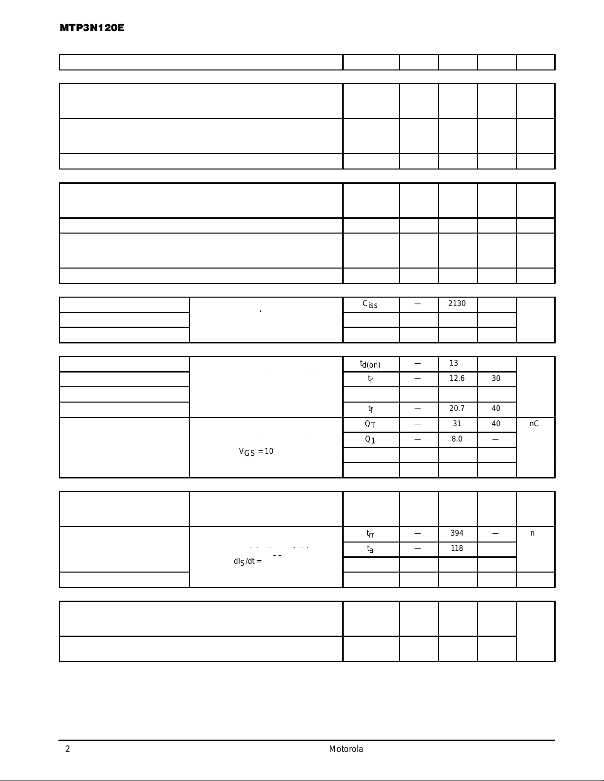
SWITCHING CHARACTERISTICS (2)
Turn–On Delay Time
t
d(on)
— 13.6 30 ns
Rise Time
t
r
— 12.6 30
Turn–Off Delay Time
VGS = 10 Vdc,
RG = 9.1 Ω)
t
d(off)
— 35.8 70
Fall Time
G
= 9.1 Ω)
t
f
— 20.7 40
Q
T
— 31 40 nC
DS
= 600 Vdc, ID = 3.0 Adc,
Q
1
— 8.0 —
(VDS = 600 Vdc, ID = 3.0 Adc,
VGS = 10 Vdc)
Q
2
— 11 —
Q
3
— 14 —
SOURCE–DRAIN DIODE CHARACTERISTICS
Forward On–Voltage
(IS = 3.0 Adc, VGS = 0 Vdc)
(IS = 3.0 Adc, VGS = 0 Vdc, TJ = 125°C)
V
SD
—
—
0.80
0.65
1.0
—
Vdc
t
rr
— 394 —
S
= 3.0 Adc, VGS = 0 Vdc,
t
a
— 118 —
(IS = 3.0 Adc, VGS = 0 Vdc,
dIS/dt = 100 A/µs)
t
b
— 276 —
Reverse Recovery Stored Charge Q
RR
— 2.11 — µC
INTERNAL PACKAGE INDUCTANCE
Internal Drain Inductance
(Measured from contact screw on tab to center of die)
(Measured from the drain lead 0.25″ from package to center of die)
L
D
—
—
3.5
4.5
—
—
Internal Source Inductance
(Measured from the source lead 0.25″ from package to source bond pad)
L
S
— 7.5 —
(1) Pulse Test: Pulse Width ≤ 300 µs, Duty Cycle ≤ 2%.
(2) Switching characteristics are independent of operating junction temperature.
Gate Charge
Reverse Recovery Time
(VDD = 600 Vdc, ID = 3.0 Adc,
(V
(I
ns
nH
MTP3N120E
3
Motorola TMOS Power MOSFET Transistor Device Data
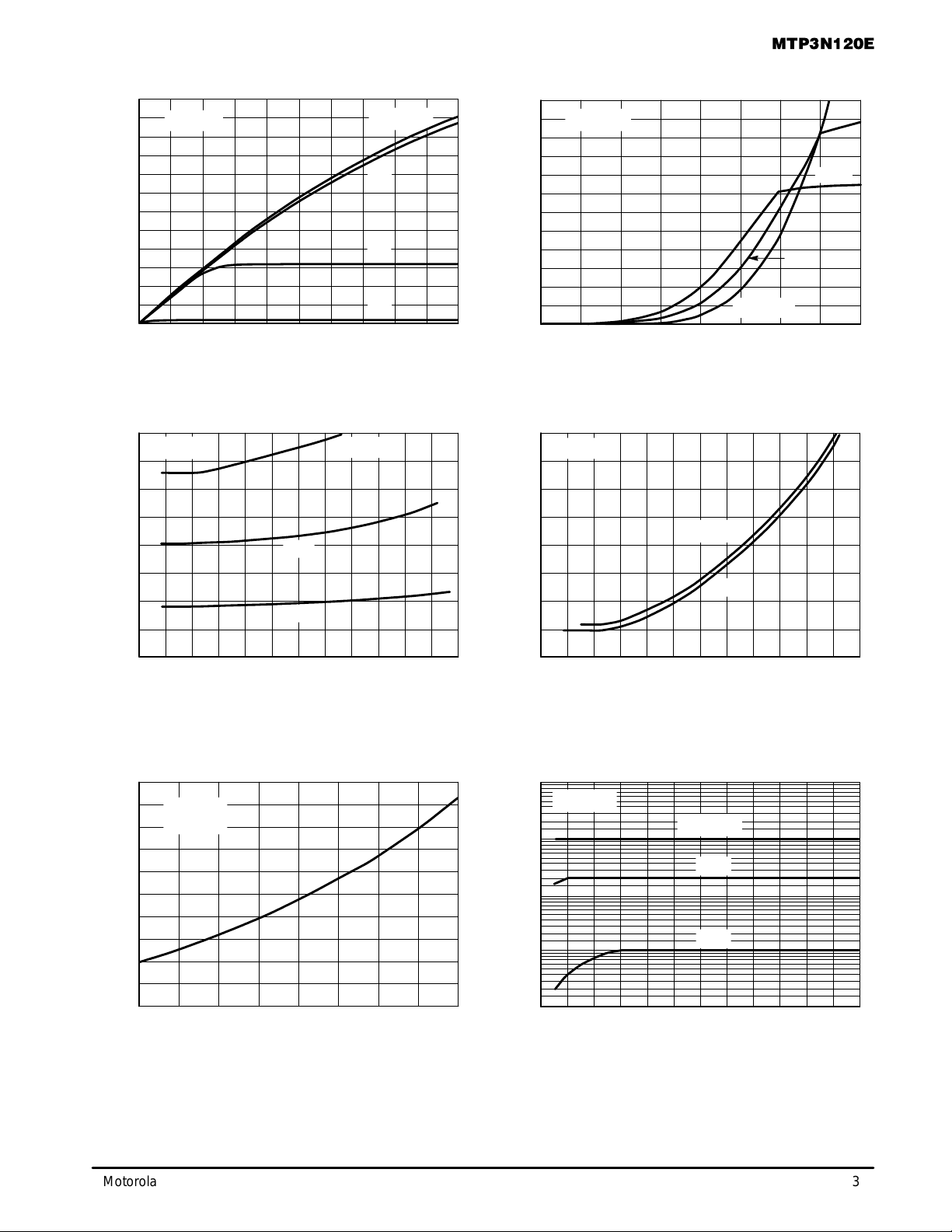
TYPICAL ELECTRICAL CHARACTERISTICS
R
DS(on)
, DRAIN–TO–SOURCE RESISTANCE
(NORMALIZED)
R
DS(on)
, DRAIN–TO–SOURCE RESISTANCE (OHMS)
R
DS(on)
, DRAIN–TO–SOURCE RESISTANCE (OHMS)
10,000
1,000
100
10
1
0 400 600 800 1000
2.5
2.0
1.5
1.0
0.5
0
–50 –25 0 25 50 75 100 125 150
5.4
5.0
4.6
4.2
3.8
ID, DRAIN CURRENT (AMPS)
8
6
4
0
0 2 4 6531
6
0
0 6 12 18 24 30
VDS, DRAIN–TO–SOURCE VOLTAGE (VOLTS)
Figure 1. On–Region Characteristics
I
D
, DRAIN CURRENT (AMPS)
I
D
, DRAIN CURRENT (AMPS)
VGS, GATE–TO–SOURCE VOLTAGE (VOLTS)
Figure 2. Transfer Characteristics
ID, DRAIN CURRENT (AMPS)
Figure 3. On–Resistance versus Drain Current
and Temperature
Figure 4. On–Resistance versus Drain Current
and Gate Voltage
TJ, JUNCTION TEMPERATURE (°C)
Figure 5. On–Resistance Variation with
Temperature
VDS, DRAIN–TO–SOURCE VOLTAGE (VOLTS)
Figure 6. Drain–To–Source Leakage
Current versus Voltage
I
DSS
, LEAKAGE (nA)
0
TJ = 25°C
VGS = 10 V
VDS ≥ 10 V
VGS = 10 V
TJ = 100°C
–55°C
TJ = 25°C
VGS = 10 V
VGS = 0 V
5
4
3
2
6
5
4
3
2
1
3.0 3.4 3.8 4.2 4.6 5.0 5.4 5.8 6.2
0 2 4 6531
TJ = 125°C
1
2
200
6 V
5 V
4 V
25°C
TJ = –55°C
100°C
25°C
VGS = 10 V
ID = 1.5 A
1200
100°C
25°C
15 V
 Loading...