

Motorola MTP1302 Datasheet

SEMICONDUCTOR TECHNICAL DATA
Order this document
by MTP1302/D
N–Channel Enhancement–Mode Silicon Gate
This advanced high cell density HDTMOS power FET is
designed to withstand high energy in the avalanche and commutation modes. This new energy efficient design also offers a
drain–to–source diode with a fast recovery time. Designed for low
voltage, high speed switching applications in power supplies,
converters and PWM motor controls, these devices are particularly
well suited for bridge circuits where diode speed and commutating
safe operating area are critical and offer additional safety margin
against unexpected voltage transients.
• Avalanche Energy Specified
• Source–to–Drain Diode Recovery Time Comparable to a
Discrete Fast Recovery Diode
• Diode Is Characterized for Use In Bridge Circuits
• I
MAXIMUM RATINGS
This document contains information on a new product. Specifications and information herein are subject to change without notice.
E–FET and HDTMOS are trademarks of Motorola, Inc. TMOS is a registered trademark of Motorola, Inc.
and V
DSS
Drain–to–Source Voltage V
Drain–to–Gate Voltage (RGS = 1.0 MΩ) V
Gate–to–Source Voltage — Continuous
Drain Current — Continuous
Drain Current — Continuous @ 100°C
Drain Current — Single Pulse (tp ≤ 10 µs)
Total Power Dissipation
Derate above 25°C
Operating and Storage Temperature Range TJ, T
Single Pulse Drain–to–Source Avalanche Energy — Starting TJ = 25°C
(VDD = 25 Vdc, VGS = 10 Vdc, Peak IL = 42 Apk, L = 0.25 mH, RG = 25 Ω)
Thermal Resistance
Junction to Case
Junction–to–Ambient
Maximum Lead Temperature for Soldering Purposes, 1/8″ from Case for 5 seconds T
Specified at Elevated Temperature
DS(on)
(TC = 25°C unless otherwise noted)
— Non–Repetitive (tp ≤ 10 ms)
Rating
Symbol Value Unit
DSS
DGR
V
V
GSM
I
I
I
DM
P
E
R
θJC
R
θJA
TMOS POWER FET
42 AMPERES
30 VOLTS
R
GS
D
D
D
stg
AS
L
= 22 m
DS(on)
CASE 221A–06
TO–220AB
30 Vdc
30 Vdc
± 20
± 20
42
20
126
74
0.592
– 55 to 150 °C
220 mJ
1.67
62.5
260 °C
W
Vdc
Vpk
Adc
Apk
Watts
W/°C
°C/W
Motorola, Inc. 1997
Motorola TMOS Power MOSFET Transistor Device Data
1

MTP1302
)
f = 1.0 MHz)
V
10 Vd
G
)
(
DS
,
D
,
(
DS
,
D
,
(
S
,
GS
,
ELECTRICAL CHARACTERISTICS
OFF CHARACTERISTICS
Drain–to–Source Breakdown Voltage
(VGS = 0 Vdc, ID = 0.25 mAdc)
Zero Gate Voltage Drain Current
(VDS = 30 Vdc, VGS = 0 Vdc)
(VDS = 30 Vdc, VGS = 0 Vdc, TJ = 125°C)
Gate–Body Leakage Current
(VGS = ± 20 Vdc, VDS = 0 Vdc)
ON CHARACTERISTICS
Gate Threshold Voltage
(VDS = VGS, ID = 250 µAdc)
Static Drain–to–Source On–Resistance
(VGS = 10 Vdc, ID = 10 Adc)
(VGS = 4.5 Vdc, ID = 5.0 Adc)
(VGS = 10 Vdc, ID = 42 Adc)
Drain–to–Source On–Voltage
(VGS = 10 Vdc, ID = 20 Adc)
(VGS = 10 Vdc, ID = 10 Adc, TJ = 150°C)
(VGS = 10 Vdc, ID = 42 Adc)
Forward Transconductance
(VDS = 10 Vdc, ID = 10 Adc)
DYNAMIC CHARACTERISTICS
Input Capacitance
Output Capacitance
Transfer Capacitance
SWITCHING CHARACTERISTICS
Turn–On Delay Time
Rise Time
Turn–Off Delay Time
Fall Time
Gate Charge
Gate Charge
SOURCE–DRAIN DIODE CHARACTERISTICS
Forward On–Voltage
Reverse Recovery Time
Reverse Recovery Stored Charge Q
(1) Pulse Test: Pulse Width ≤300 µs, Duty Cycle ≤ 2%.
(2) Switching characteristics are independent of operating junction temperature.
(1)
(TJ = 25°C unless otherwise noted)
Characteristic Symbol Min Typ Max Unit
(VDS = 25 Vdc, VGS = 0 Vdc,
(2)
(IS = 20 Adc, VGS = 0 Vdc, TJ = 125°C)
f = 1.0 MHz
(VDD = 15 Vdc, ID = 20 Adc,
GS
RG = 9.1 Ω)
(VDS = 24 Vdc, ID = 20 Adc,
VGS = 5.0 Vdc)
(VDS = 24 Vdc, ID = 20 Adc,
VGS = 10 Vdc)
(IS = 20 Adc, VGS = 0 Vdc)
(IS = 20 Adc, VGS = 0 Vdc,
dIS/dt = 100 A/µs)
=
c,
V
(BR)DSS
I
DSS
I
GSS
V
GS(th)
R
DS(on)
V
DS(on)
g
FS
C
iss
C
oss
C
rss
t
d(on)
t
r
t
d(off)
t
f
Q
Q
Q
Q
Q
Q
Q
Q
V
SD
t
rr
t
a
t
b
RR
30 — —
—
—
— — 100
1.0 1.5 2.0
—
—
—
—
—
—
10 16 —
— 755 1162 pF
— 370 518
— 102 204
— 7.2 15
— 52 104
— 45 90
— 73 146
T
1
2
3
T
1
2
3
— 14.5 21.8
— 2.2 —
— 8.8 —
— 6.8 —
— 27 40.5
— 2.2 —
— 10 —
— 7.2 —
—
—
— 38 —
— 19 —
— 20 —
— 36 — µC
—
—
19
26
19.5
0.38
—
0.82
0.83
0.79
10
100
22
29
—
0.5
0.33
—
1.1
—
Vdc
µAdc
nAdc
Vdc
m
W
Vdc
Mhos
ns
nC
nC
Vdc
ns
2
Motorola TMOS Power MOSFET Transistor Device Data
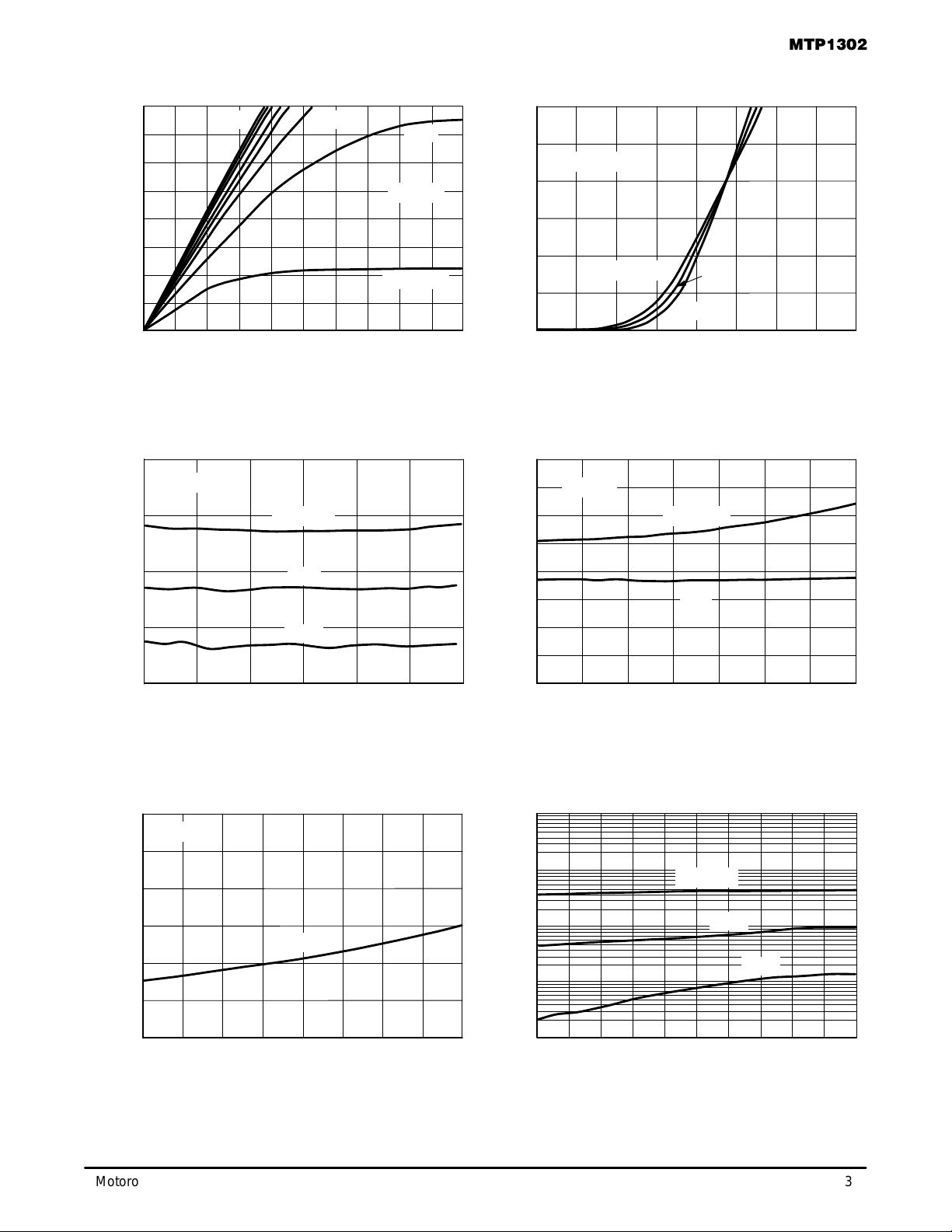
TYPICAL ELECTRICAL CHARACTERISTICS
MTP1302
40
35
30
25
20
15
, DRAIN CURRENT (AMPS)R
10
D
I
5.0
0
0.4 0.8 1.2
0.2 0.6 1.81.6 2.01.4
VDS, DRAIN–TO–SOURCE VOL TAGE (VOLTS)
5.0 V10 V
4.0 V
TJ = 25°C
VGS = 3.0 V
1.00
30
25
20
15
10
, DRAIN CURRENT (AMPS)
D
I
5.0
0
VDS ≥ 10 V
TJ = 125°C
1.5 2.0 5.0
VGS, GATE–T O–SOURCE VOLT AGE (VOLTS)
2.51.0
–55°C
25°C
4.0
4.53.0 3.5
Figure 1. On–Region Characteristics Figure 2. Transfer Characteristics
0.03
VGS = 10 V
TJ = 100°C
0.04
0.035
0.03
0.025
TJ = 25°C
VGS = 4.5 V
0.02
, DRAIN–TO–SOURCE ON–RESISTANCE (OHMS)
0.01
10 20 30
DS(on)
15 25 35
ID, DRAIN CURRENT (AMPS)
Figure 3. On–Resistance versus
Drain Current and Temperature
3.0
ID = 20 A
2.0
VGS = 10 V
1.0
25°C
–55°C
, DRAIN–TO–SOURCE ON–RESISTANCE (OHMS)
40
R
, LEAKAGE (nA)
I
0.02
0.015
0.01
0.005
0
DS(on)
1000
100
10
DSS
1.0
10 V
15 20 30
25 35
ID, DRAIN CURRENT (AMPS)
40
Figure 4. On–Resistance versus Drain Current
and Gate Voltage
TJ = 125°C
100°C
25°C
4510
, DRAIN–TO–SOURCE RESIST ANCE (NORMALIZED)R
0
DS(on)
–25–50
0
TJ, JUNCTION TEMPERATURE (
5025 10 3015
75 100 150125
°
C)
Figure 5. On–Resistance Variation with
T emperature
Motorola TMOS Power MOSFET Transistor Device Data
0.1
5.0 20
VDS, DRAIN–TO–SOURCE VOL TAGE (VOLTS)
Figure 6. Drain–T o–Source Leakage
Current versus Voltage
25
3
 Loading...