

1
Motorola TMOS Power MOSFET Transistor Device Data
P–Channel Enhancement–Mode Silicon Gate
This TMOS Power FET is designed for medium voltage, high
speed power switching applications such as switching regulators,
converters, solenoid and relay drivers.
• Silicon Gate for Fast Switching Speeds — Switching Times
Specified at 100°C
• Designer’s Data — I
DSS
, V
DS(on)
, V
GS(th)
and SOA Specified
at Elevated Temperature
• Rugged — SOA is Power Dissipation Limited
• Source–to–Drain Diode Characterized for Use With Inductive Loads
MAXIMUM RATINGS
(TC = 25°C unless otherwise noted)
Rating
Symbol Value Unit
Drain–Source Voltage V
DSS
100 Vdc
Drain–Gate Voltage (RGS = 1.0 MΩ) V
DGR
100 Vdc
Gate–Source Voltage — Continuous
Gate–Source Voltage — Non–repetitive (tp ≤ 50 µs)
V
GS
V
GSM
±20
±40
Vdc
Vpk
Drain Current — Continuous
Drain Current — Pulsed
I
D
I
DM
12
28
Adc
Total Power Dissipation
Derate above 25°C
P
D
75
0.6
Watts
W/°C
Operating and Storage Temperature Range TJ, T
stg
–65 to 150 °C
THERMAL CHARACTERISTICS
Thermal Resistance — Junction to Case
Thermal Resistance — Junction to Ambient°
R
θJC
R
θJA
1.67
62.5
°C/W
Maximum Lead Temperature for Soldering Purposes, 1/8″ from case for 10 seconds T
L
260 °C
Designer’s Data for “Worst Case” Conditions — The Designer’s Data Sheet permits the design of most circuits entirely from the information presented. SOA Limit
curves — representing boundaries on device characteristics— are given to facilitate “worst case” design.
Designer’s is a trademark of Motorola, Inc.
REV 1
Order this document
by MTP12P10/D
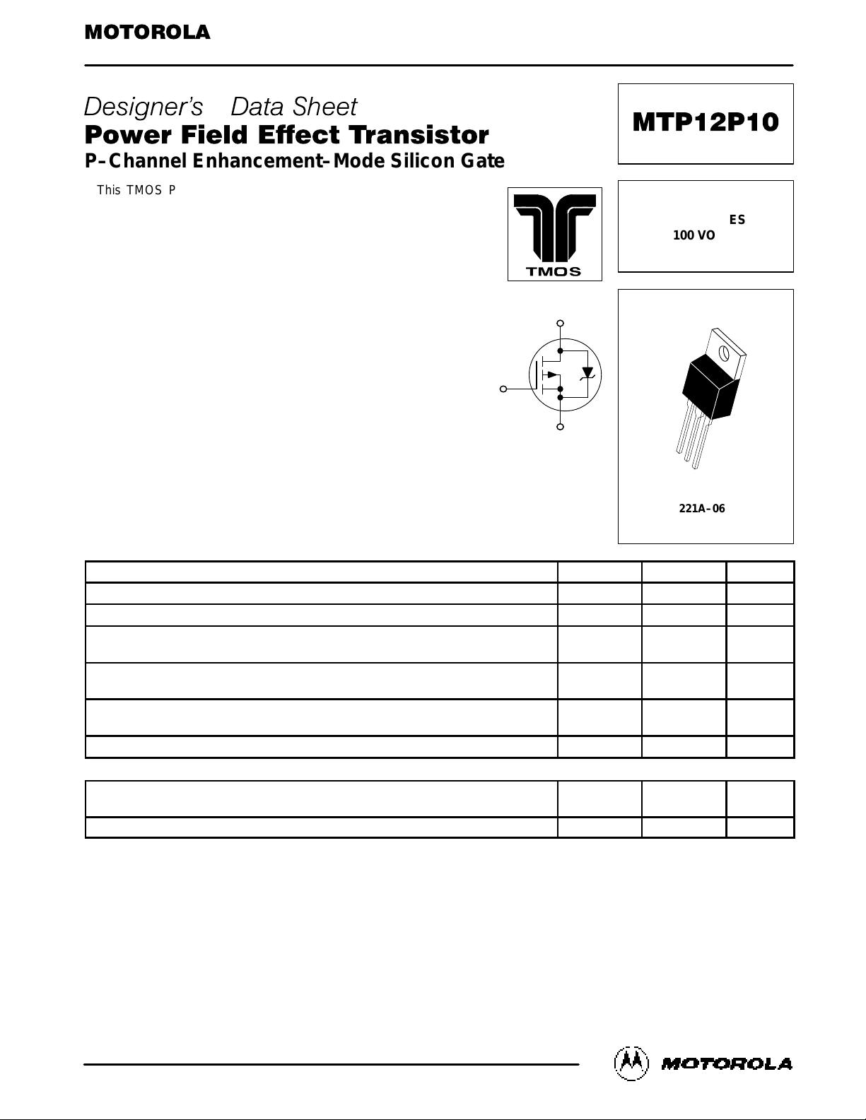
SEMICONDUCTOR TECHNICAL DATA
TMOS POWER FET
12 AMPERES
100 VOLTS
R
DS(on)
= 0.3 OHM
D
S
G
CASE 221A–06, Style 5
TO–220AB
Motorola, Inc. 1996
MTP12P10
2
Motorola TMOS Power MOSFET Transistor Device Data
ELECTRICAL CHARACTERISTICS
(T
J
= 25°C unless otherwise noted)
Characteristic
Symbol Min Max Unit
OFF CHARACTERISTICS
Drain–Source Breakdown Voltage
(VGS = 0, ID = 0.25 mA)
V
(BR)DSS
100 — Vdc
Zero Gate Voltage Drain Current
(VDS = Rated V
DSS
, VGS = 0)
(VDS = Rated V
DSS
, VGS = 0, TJ = 125°C)
I
DSS
—
—
10
100
µAdc
Gate–Body Leakage Current, Forward (V
GSF
= 20 Vdc, VDS = 0) I
GSSF
— 100 nAdc
Gate–Body Leakage Current, Reverse (V
GSR
= 20 Vdc, VDS = 0) I
GSSR
— 100 nAdc
ON CHARACTERISTICS*
Gate Threshold Voltage (VDS = VGS, ID = 1.0 mA)
TJ = 100°C
V
GS(th)
2.0
1.5
4.5
4.0
Vdc
Static Drain–Source On–Resistance (VGS = 10 Vdc, ID = 6.0 Adc) R
DS(on)
— 0.3 Ohm
Drain–Source On–Voltage (VGS = 10 V)
(ID = 12 Adc)
(ID = 6.0 Adc, TJ = 100°C)
V
DS(on)
—
—
4.2
3.8
Vdc
Forward Transconductance (VDS = 15 V, ID = 6.0 A) g
FS
2.0 — mhos
DYNAMIC CHARACTERISTICS
Input Capacitance
C
iss
— 920 pF
Output Capacitance
(VDS = 25 V, VGS = 0,
f = 1.0 MHz)
C
oss
— 575
Reverse Transfer Capacitance
See Figure 10
C
rss
— 200
SWITCHING CHARACTERISTICS* (TJ = 100°C)
Turn–On Delay Time
t
d(on)
— 50 ns
Rise Time
t
r
— 150
Turn–Off Delay Time
RG = 50 Ω)
See Figures 12 and 13
t
d(off)
— 150
Fall Time t
f
— 150
Total Gate Charge
Q
g
33 (Typ) 50 nC
Gate–Source Charge
(VDS = 0.8 Rated V
DSS
,
ID = Rated ID, VGS = 10 V)
Q
gs
16 (Typ) —
Gate–Drain Charge
See Figure 11
Q
gd
17 (Typ) —
SOURCE–DRAIN DIODE CHARACTERISTICS*
Forward On–Voltage
V
SD
4.0 (Typ) 5.5 Vdc
Forward Turn–On Time
(IS = Rated ID,
V
= 0)
t
on
Limited by stray inductance
Reverse Recovery Time
VGS = 0)
t
rr
300 (Typ) — ns
INTERNAL PACKAGE INDUCTANCE (TO–204)
Internal Drain Inductance
(Measured from the contact screw on the header closer
to the source pin and the center of the die)
L
d
5.0 (Typ) —
Internal Source Inductance
(Measured from the source pin, 0.25″ from the package
to the source bond pad)
L
s
12.5 (Typ) —
INTERNAL PACKAGE INDUCTANCE (TO–220)
Internal Drain Inductance
(Measured from the contact screw on tab to center of die)
(Measured from the drain lead 0.25″ from package to center of die)
L
d
3.5 (Typ)
4.5 (Typ)
—
—
Internal Source Inductance
(Measured from the source lead 0.25″ from package to source bond pad)
L
s
7.5 (Typ) —
*Pulse Test: Pulse Width ≤ 300 µs, Duty Cycle ≤ 2%.
(VDD = 25 V, ID = 0.5 Rated ID,
nH
nH
 Loading...