

Motorola MTE53N50E Datasheet
SEMICONDUCTOR TECHNICAL DATA
Order this document
by MTE53N50E/D
Motorola Preferred Device
N–Channel Enhancement–Mode Silicon Gate
This advanced high voltage TMOS E–FET is designed to
withstand high energy in the avalanche mode and switch efficiently .
This new high energy device also offers a drain–to–source diode
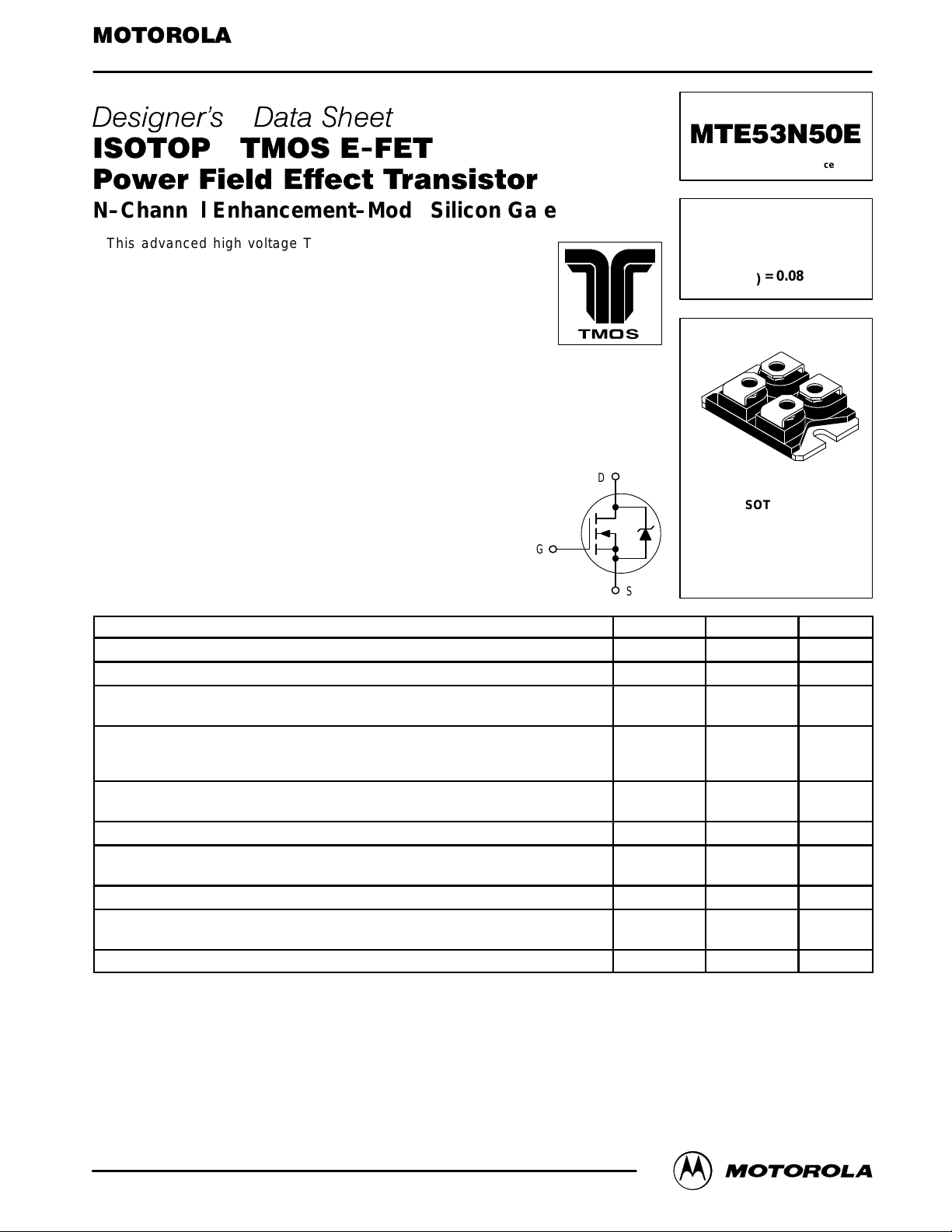
TMOS POWER FET
53 AMPERES
500 VOL TS
R
DS(on)
= 0.080 OHM
with fast recovery time. Designed for high voltage, high speed
switching applications such as power supplies, PWM motor
controls and other inductive loads, the avalanche energy capability
is specified to eliminate the guesswork in designs where inductive
loads are switched and offer additional safety margin against
unexpected voltage transients.
• 2500 V RMS Isolated Isotop Package
• Avalanche Energy Specified
1
4
3
2
• Source–to–Drain Diode Recovery Time Comparable to a Discrete
Fast Recovery Diode
• Diode is Characterized for Use in Bridge Circuits
• Very Low Internal Parasitic Inductance
• I
DSS
and V
Specified at Elevated Temperature
DS(on)
• U. L. Recognized, File #E69369
G
MAXIMUM RATINGS
Drain–Source Voltage V
Drain–Gate Voltage (RGS = 1.0 MΩ) V
Gate–Source Voltage — Continuous
Gate–Source Voltage — Non–Repetitive (tp ≤ 10 ms)
Drain Current — Continuous
Drain Current — Continuous @ 100°C
Drain Current — Single Pulse (tp ≤ 10 µs)
Total Power Dissipation
Derate above 25°C
Operating and Storage Temperature Range TJ, T
Single Pulse Drain–to–Source Avalanche Energy
(VDD = 25 Vdc, VGS = 10 Vdc, IL= 53 Apk, L = 0.29 mH, RG =25Ω)
RMS Isolation Voltage V
Thermal Resistance — Junction to Case
Thermal Resistance — Junction to Ambient
Maximum Lead Temperature for Soldering Purposes, 1/8″ from case for 10 seconds T
Designer’s Data for “Worst Case” Conditions — The Designer’s Data Sheet permits the design of most circuits entirely from the information presented. SOA Limit
curves — representing boundaries on device characteristics — are given to facilitate “worst case” design.
E–FET is a trademark of Motorola, Inc. TMOS is a registered trademark of Motorola, Inc.
ISOTOP is a trademark of SGS–THOMSON Microelectronics.
(TC = 25°C unless otherwise noted)
Rating
D
SOT–227B
1. Source
2. Gate
3. Drain
S
Symbol Value Unit
DSS
DGR
V
GS
V
GSM
I
D
I
D
I
DM
P
D
stg
E
AS
ISO
R
θJC
R
θJA
L
4. Source 2
500 Vdc
500 Vdc
± 20
± 40
53
33
210
460
3.70
–40 to 150 °C
400
2500 Vac
0.28
62.5
260 °C
Vdc
Vpk
Adc
Watts
W/°C
mJ
°C/W
Preferred devices are Motorola recommended choices for future use and best overall value.
REV 2
Motorola TMOS Power MOSFET Transistor Device Data
Motorola, Inc. 1996
1
MTE53N50E
)
f = 1.0 MHz)
V
G
)
(
DS
,
D
,
(
S
,
GS
,
ELECTRICAL CHARACTERISTICS
OFF CHARACTERISTICS
Drain–Source Breakdown Voltage
(VGS = 0 Vdc, ID = 250 µAdc)
T emperature Coef ficient (Positive)
Zero Gate Voltage Drain Current
(VDS = 500 Vdc, VGS = 0 Vdc)
(VDS = 500 Vdc, VGS = 0 Vdc, TJ = 125°C)
Gate–Body Leakage Current (VGS = ± 20 Vdc, VDS = 0) I
ON CHARACTERISTICS (1)
Gate Threshold Voltage
(VDS = VGS, ID = 250 µAdc)
Threshold Temperature Coefficient (Negative)
Static Drain–Source On–Resistance (VGS = 10 Vdc, ID = 26.5 Adc) R
Drain–Source On–Voltage (VGS = Vdc)
(ID = 53 Adc)
(ID = 26.5 Adc, TJ = 125°C)
Forward Transconductance (VDS = 15 Vdc, ID = 26.5 Adc) g
DYNAMIC CHARACTERISTICS
Input Capacitance
Output Capacitance
Reverse Transfer Capacitance
SWITCHING CHARACTERISTICS (2)
Turn–On Delay Time
Rise Time
Turn–Off Delay Time
Fall Time
Gate Charge
SOURCE–DRAIN DIODE CHARACTERISTICS
Forward On–Voltage (1)
Reverse Recovery Time
Reverse Recovery Stored Charge Q
INTERNAL PACKAGE INDUCTANCE
Internal Drain Inductance
(Measured from contact screw on tab to center of die)
(Measured from the drain lead 0.25″ from package to center of die)
Internal Source Inductance
(Measured from the source lead 0.25″ from package to center of die)
(1) Pulse Test: Pulse Width ≤ 300 µs, Duty Cycle ≤ 2%.
(2) Switching characteristics are independent of operating junction temperature.
(T
= 25°C unless otherwise noted)
J
Characteristic
(VDS = 25 Vdc, VGS = 0 Vdc,
(VDD = 250 Vdc, ID = 53 Adc,
(VDS = 400 Vdc, ID = 53 Adc,
(IS = 53 Adc, VGS = 0 Vdc, TJ = 125°C)
f = 1.0 MHz
= 10 Vdc,
GS
RG = 4.7 Ω)
VGS = 10 Vdc)
(IS = 53 Adc, VGS = 0 Vdc)
(IS = 53 Adc, VGS = 0 Vdc,
dIS/dt = 100 A/µs)
Symbol Min Typ Max Unit
V
(BR)DSS
I
DSS
GSS
V
GS(th)
DS(on)
V
DS(on)
FS
C
iss
C
oss
C
rss
t
d(on)
t
r
t
d(off)
t
f
Q
T
Q
1
Q
2
Q
3
V
SD
t
rr
t
a
t
b
RR
L
D
L
S
500
—
—
—
— — 200 nAdc
2.0
—
— 63 80 mOhm
—
—
25 45 — mhos
— 14400 — pF
— 1560 —
— 240 —
— 67 — ns
— 322 —
— 362 —
— 310 —
— 474 700 nC
— 86 —
— 206 —
— 148 —
—
—
— 720 —
— 460 —
— 260 —
— 15 — µC
—
—
— 5.0 — nH
560
550
—
—
3.2
—
—
—
0.95
0.90
3.5
5.0
—
—
10
100
4.0
—
4.8
4.3
1.3
—
—
—
mV/°C
mV/°C
Vdc
µAdc
Vdc
Vdc
Vdc
ns
nH
2
Motorola TMOS Power MOSFET Transistor Device Data
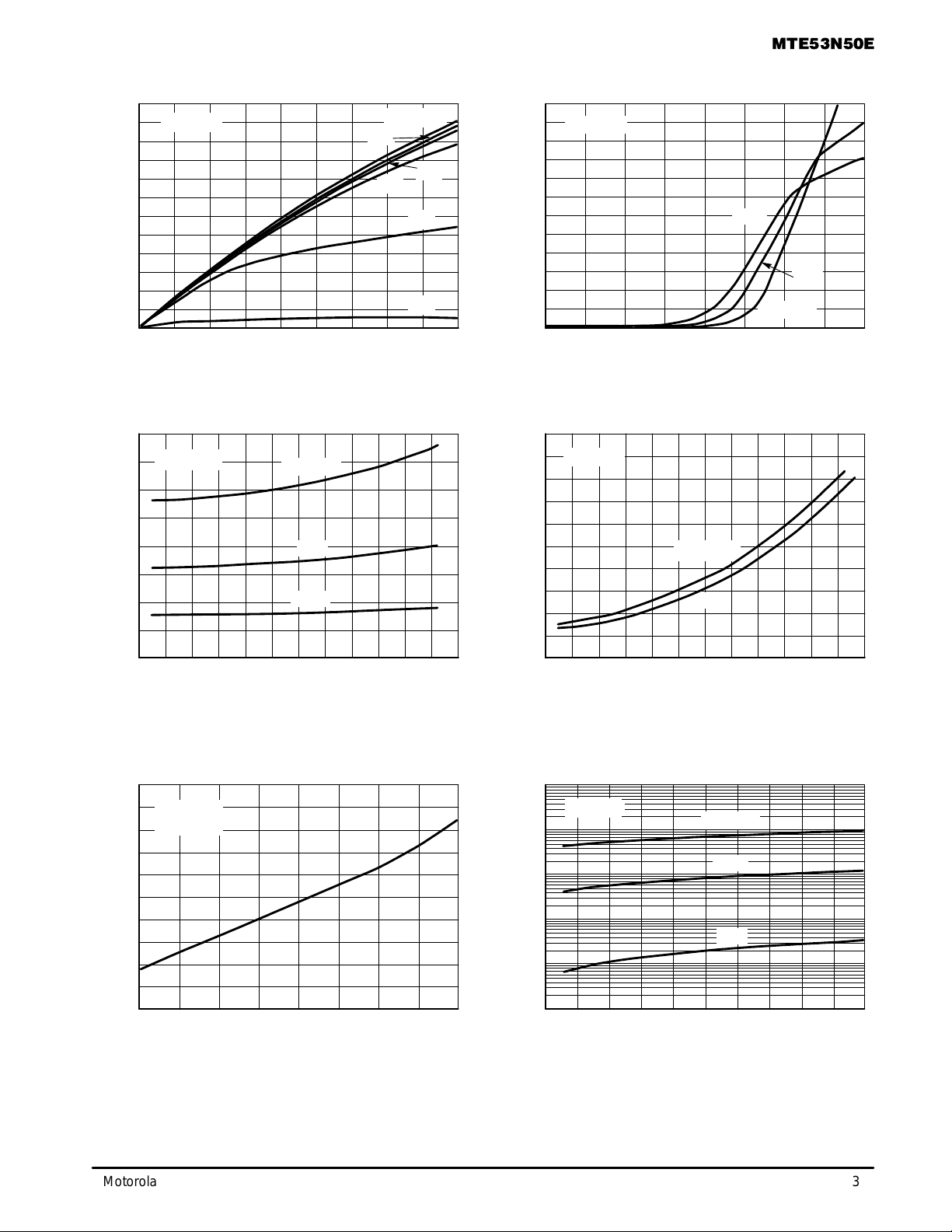
TYPICAL ELECTRICAL CHARACTERISTICS
MTE53N50E
120
100
80
60
40
, DRAIN CURRENT (AMPS)
D
I
20
0
0
0.16
0.12
0.08
TJ = 25°C
135
VDS, DRAIN–TO–SOURCE VOL TAGE (VOLTS)
VGS = 10 V
8 V
6 V
Figure 1. On–Region Characteristics
VGS = 10 V
TJ = 100°C
25°C
5 V
4 V
8
7 V
120
V
≥ 10 V
100
80
60
40
, DRAIN CURRENT (AMPS)
D
I
20
97642
DS
100°C
25°C
0
34
VGS, GATE–T O–SOURCE VOLTAGE (VOLTS)
TJ = –55°C
652
Figure 2. Transfer Characteristics
0.085
TJ = 25°C
0.08
0.075
VGS = 10 V
0.07
0.04
, DRAIN–TO–SOURCE RESIST ANCE (OHMS)
0
DS(on)
R
0 40 60 80 100 120
20
ID, DRAIN CURRENT (AMPS)
–55°C
Figure 3. On–Resistance versus Drain Current
and T emperature
2.5
VGS = 10 V
ID = 26.5 A
2
1.5
1
(NORMALIZED)
, DRAIN–TO–SOURCE RESIST ANCE
0.5
DS(on)
R
0
–50 0 50 100 150
–25 25 75
TJ, JUNCTION TEMPERATURE (°C)
125
0.065
, DRAIN–TO–SOURCE RESIST ANCE (OHMS)
0.06
DS(on)
R
ID, DRAIN CURRENT (AMPS)
15 V
6040200 80 120
Figure 4. On–Resistance versus Drain Current
and Gate Voltage
100000
VGS = 0 V
10000
1000
, LEAKAGE (nA)
100
DSS
I
10
1
0 100 300200 400 500
VDS, DRAIN–TO–SOURCE VOL TAGE (VOLTS)
TJ = 125°C
100°C
25°C
100
Figure 5. On–Resistance Variation with
Temperature
Motorola TMOS Power MOSFET Transistor Device Data
Figure 6. Drain–T o–Source Leakage Current
versus V oltage
3
 Loading...