

Motorola MTE30N50E Datasheet
1
Motorola TMOS Power MOSFET Transistor Device Data
N–Channel Enhancement–Mode Silicon Gate
This advanced TMOS E–FET is designed to withstand high
energy in t he avalanche mode and switch efficiently. This new
energy d esign also offers a d rain–to–source d iode w ith fast
recovery time. Designed for high voltage, high speed switching
applications in power supplies, PWM motor controls, and other
inductive loads. The avalanche energy capability is specified to
eliminate the guesswork in designs where i nductive loads are
switched and offer additional safety margin against unexpected
voltage transients.
• 2500 V RMS Isolated ISOTOP Package
• Avalanche Energy Specified
• Source–to–Drain Diode Recovery Time Comparable to a Discrete
Fast Recovery Diode
• Diode is Characterized for Use in Bridge Circuits
• Very Low Internal Parasitic Inductance
• I
DSS
and V
DS(on)
Specified at Elevated Temperature
• U.L. Recognized, File #E69369
MAXIMUM RATINGS
(TC = 25°C unless otherwise noted)
Rating
Symbol Value Unit
Drain–to–Source Voltage V
DSS
500 Vdc
Drain–to–Gate Voltage (RGS = 1.0 MΩ) V
DGR
500 Vdc
Gate–to–Source Voltage — Continuous
— Non–Repetitive (tp ≤ 10 ms)
V
GS
V
GSM
± 20
± 40
Vdc
Vpk
Drain Current — Continuous @ 25°C
Drain Current — Continuous @ 100°C
Drain Current — Single Pulse (tp ≤ 10 µs)
I
D
I
D
I
DM
30
12
80
Adc
Apk
Total Power Dissipation @ 25°C
Derate above 25°C
P
D
250
2.0
Watts
W/°C
Operating and Storage Temperature Range TJ, T
stg
–55 to 150 °C
Single Pulse Drain–to–Source Avalanche Energy – Starting TJ = 25°C
(VDD = 100 Vdc, VGS = 10 Vdc, Peak IL= 30 Apk, L = 10 mH, RG = 25 Ω)
E
AS
3000
mJ
Thermal Resistance — Junction to Case
Thermal Resistance — Junction to Ambient
R
θJC
R
θJA
0.5
62.5
°C/W
Maximum Lead Temperature for Soldering Purposes, 1/8″ from case for 10 seconds T
L
260 °C
This document contains information on a new product. Specifications and information herein are subject to change without notice.
E–FET is a trademark of Motorola, Inc. TMOS is a registered trademark of Motorola, Inc.
ISOTOP is a trademark of SGS–THOMSON Microelectronics.
Preferred devices are Motorola recommended choices for future use and best overall value.
Order this document
by MTE30N50E/D
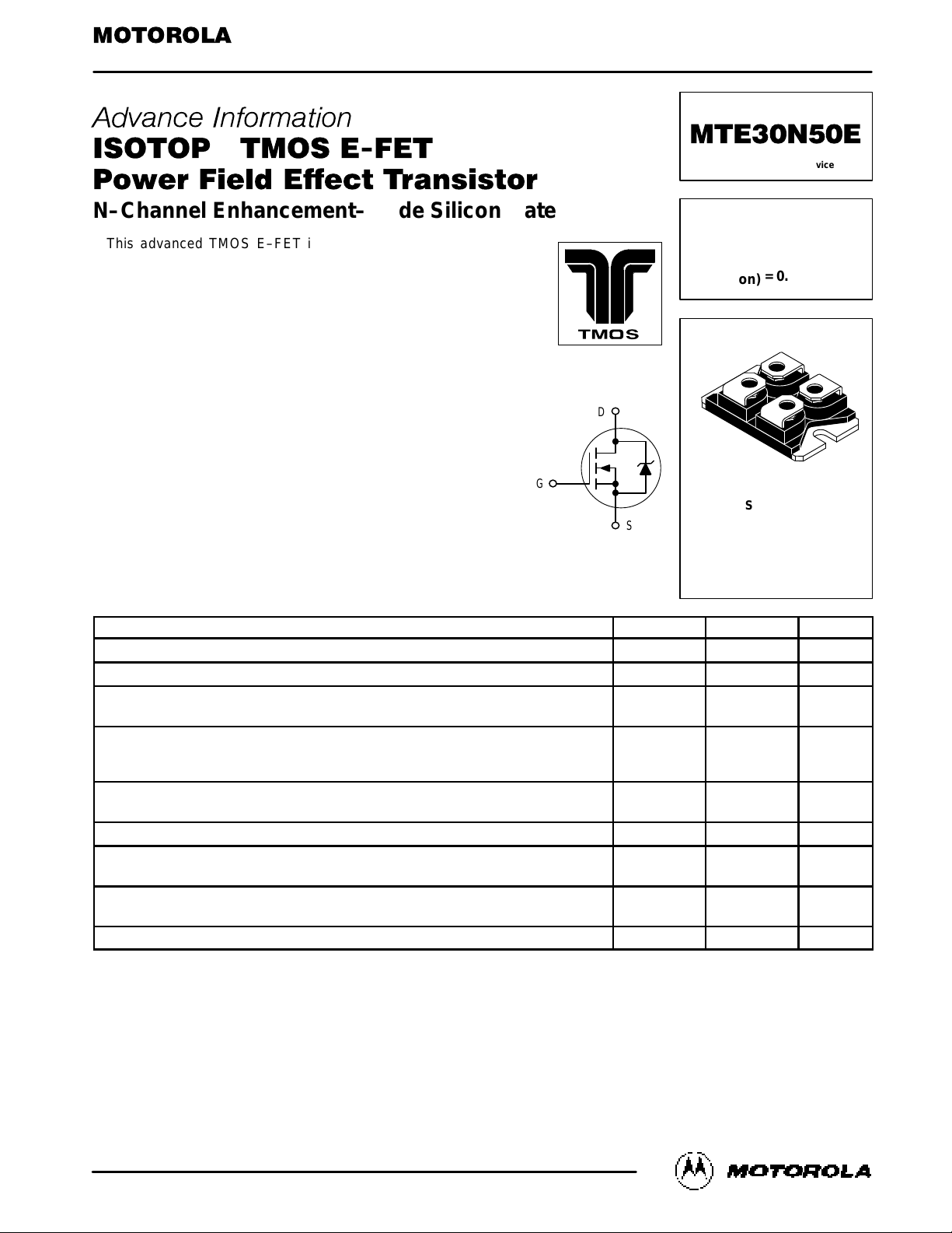
SEMICONDUCTOR TECHNICAL DATA
TMOS POWER FET
30 AMPERES
500 VOLTS
R
DS(on)
= 0.150 OHM
Motorola Preferred Device
D
S
G
SOT–227B
1
2
3
4
1. Source
2. Gate
3. Drain
4. Source 2
Motorola, Inc. 1996
MTE30N50E
2
Motorola TMOS Power MOSFET Transistor Device Data
ELECTRICAL CHARACTERISTICS
(T
J
= 25°C unless otherwise noted)
Characteristic
Symbol Min Typ Max Unit
OFF CHARACTERISTICS
Drain–to–Source Breakdown Voltage
(VGS = 0 Vdc, ID = 0.25 mAdc)
Temperature Coefficient (Positive)
V
(BR)DSS
500
—
560
566
—
—
Vdc
mV/°C
Zero Gate Voltage Drain Current
(VDS = 500 Vdc, VGS = 0 Vdc)
(VDS = 500 Vdc, VGS = 0 Vdc, TJ = 125°C)
I
DSS
—
—
—
—
10
200
µAdc
Gate–Body Leakage Current (VGS = ± 20 Vdc, VDS = 0) I
GSS
— — 100 nAdc
ON CHARACTERISTICS (1)
Gate Threshold Voltage
(VDS = VGS, ID = 250 µAdc)
Threshold Temperature Coefficient (Negative)
V
GS(th)
2.0
—
3.2
7.0
4.0
—
Vdc
mV/°C
Static Drain–to–Source On–Resistance (VGS = 10 Vdc, ID = 15 Adc) R
DS(on)
— 0.13 0.15 Ohms
Drain–to–Source On–Voltage
(VGS = 10 Vdc, ID = 30 Adc)
(VGS = 10 Vdc, ID = 15 Adc)
V
DS(on)
—
—
4.1
—
5.0
7.0
Vdc
Forward Transconductance (VDS = 15 Vdc, ID = 15 Adc) g
FS
17 — — mhos
DYNAMIC CHARACTERISTICS
Input Capacitance
C
iss
— 7200 10080 pF
Output Capacitance
(VDS = 25 Vdc, VGS = 0 Vdc,
f = 1.0 MHz)
C
oss
— 775 1200
Transfer Capacitance
f = 1.0 MHz)
C
rss
— 120 250
SWITCHING CHARACTERISTICS (2)
Turn–On Delay Time
t
d(on)
— 32 60 ns
Rise Time
t
r
— 105 175
Turn–Off Delay Time
VGS = 10 Vdc,
RG = 4.7 Ω)
t
d(off)
— 160 275
Fall Time
G
= 4.7 Ω)
t
f
— 115 200
Q
T
— 235 350 nC
(see figure 8)
DS
= 400 Vdc, ID = 30 Adc,
Q
1
— 35 —
(VDS = 400 Vdc, ID = 30 Adc,
VGS = 10 Vdc)
Q
2
— 110 —
Q
3
— 65 —
SOURCE–DRAIN DIODE CHARACTERISTICS
Forward On–Voltage
(IS = 30 Adc, VGS = 0 Vdc)
(IS = 30 Adc, VGS = 0 Vdc, TJ = 125°C)
V
SD
—
—
0.95
0.88
1.2
—
Vdc
t
rr
— 485 —
S
= 30 Adc, VGS = 0 Vdc,
t
a
— 312 —
(IS = 30 Adc, VGS = 0 Vdc,
dIS/dt = 100 A/µs)
t
b
— 173 —
Reverse Recovery Stored Charge Q
RR
— 8.2 — µC
INTERNAL PACKAGE INDUCTANCE
Internal Drain Inductance L
D
— 5.0 — nH
Internal Source Inductance L
S
— 5.0 — nH
(1) Pulse Test: Pulse Width ≤ 300 µs, Duty Cycle ≤ 2%.
(2) Switching characteristics are independent of operating junction temperature.
Gate Charge
Reverse Recovery Time
(VDD = 250 Vdc, ID = 30 Adc,
(V
(I
ns
MTE30N50E
3
Motorola TMOS Power MOSFET Transistor Device Data
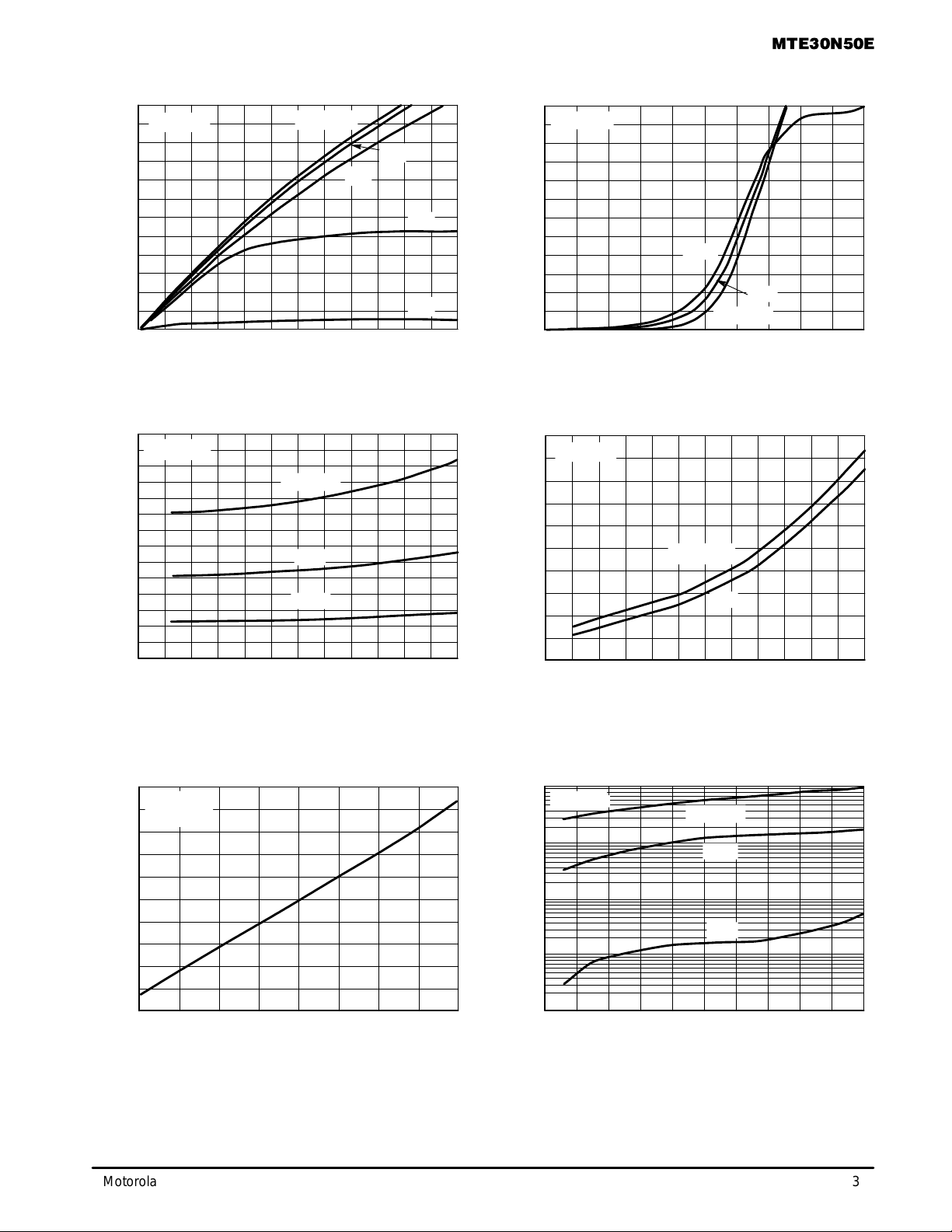
TYPICAL ELECTRICAL CHARACTERISTICS
R
DS(on)
, DRAIN–TO–SOURCE RESISTANCE
(NORMALIZED)
R
DS(on)
, DRAIN–TO–SOURCE RESISTANCE (OHMS)
0
VDS, DRAIN–TO–SOURCE VOLTAGE (VOLTS)
Figure 1. On–Region Characteristics
I
D
, DRAIN CURRENT (AMPS)
I
D
, DRAIN CURRENT (AMPS)
VGS, GATE–TO–SOURCE VOLTAGE (VOLTS)
Figure 2. Transfer Characteristics
ID, DRAIN CURRENT (AMPS)
Figure 3. On–Resistance versus Drain Current
and Temperature
ID, DRAIN CURRENT (AMPS)
Figure 4. On–Resistance versus Drain Current
and Gate Voltage
TJ, JUNCTION TEMPERATURE (°C)
Figure 5. On–Resistance Variation with
Temperature
VDS, DRAIN–TO–SOURCE VOLTAGE (VOLTS)
Figure 6. Drain–To–Source Leakage Current
versus Voltage
TJ = 25°C
VGS = 10 V
VGS = 10 V
ID = 15 A
8 V
6 V
–50 0 50 100 150
60
40
20
10
0
121062
60
40
30
0
652
50
20
3020100 40 60
0 100 300200 400 500
5 V
4 V
125
4 8
10
3 4
VDS ≥ 10 V
100°C
25°C
TJ = –55°C
0.2
0.15
0.1
0.5
0
0 20 30 40 50 60
TJ = 100°C
25°C
–55°C
0.17
0.16
0.15
0.14
0.13
0.12
VGS = 10 V
TJ = 25°C
VGS = 10 V
15 V
R
DS(on)
, DRAIN–TO–SOURCE RESISTANCE (OHMS)
–25 25 75
2.5
2
1.5
1
0.5
0
I
DSS
, LEAKAGE (nA)
10000
1000
100
10
1
VGS = 0 V
TJ = 125°C
100°C
25°C
50
30
10
50
76.55.52.5 3.5 4.5
0.25
0.3
0.35
 Loading...