

Motorola MTD15N06V Datasheet
1
Motorola TMOS Power MOSFET Transistor Device Data
!
N–Channel Enhancement–Mode Silicon Gate
TMOS V is a new technology designed to achieve an on–resistance area product about one–half that of standard MOSFET s. This
new technology more than doubles the present cell density of our
50 and 60 volt TMOS devices. Just as with our TMOS E–FET
designs, TMOS V is designed to withstand high energy in the
avalanche and commutation modes. Designed for low voltage, high
speed switching applications in power supplies, converters and
power motor controls, these devices are particularly well suited for
bridge circuits where diode speed and commutating safe operating
areas are critical and offer additional safety margin against
unexpected voltage transients.
New Features of TMOS V
• On–resistance Area Product about One–half that of Standard
MOSFETs with New Low Voltage, Low R
DS(on)
Technology
• Faster Switching than E–FET Predecessors
Features Common to TMOS V and TMOS E–FETS
• Avalanche Energy Specified
• I
DSS
and V
DS(on)
Specified at Elevated Temperature
• Static Parameters are the Same for both TMOS V and TMOS E–FET
• Surface Mount Package Available in 16 mm 13–inch/2500 Unit Tape & Reel, Add T4 Suffix to Part Number
MAXIMUM RATINGS
(TC = 25°C unless otherwise noted)
Rating
Symbol Value Unit
Drain–Source Voltage V
DSS
60 Vdc
Drain–Gate Voltage (RGS = 1.0 MΩ) V
DGR
60 Vdc
Gate–Source Voltage — Continuous
Gate–Source Voltage — Single Pulse (tp ≤ 50 ms)
V
GS
V
GSM
± 20
± 25
Vdc
Vpk
Drain Current — Continuous @ 25°C
Drain Current — Continuous @ 100°C
Drain Current — Single Pulse (tp ≤ 10 µs)
I
D
I
D
I
DM
15
8.7
45
Adc
Apk
Total Power Dissipation @ 25°C
Derate above 25°C
Total Power Dissipation @ TA = 25°C, when mounted to minimum recommended pad size
P
D
55
0.36
2.1
Watts
W/°C
Watts
Operating and Storage Temperature Range TJ, T
stg
–55 to 175 °C
Single Pulse Drain–to–Source Avalanche Energy — Starting TJ = 25°C
(VDD = 25 Vdc, VGS = 10 Vdc, IL = 15 Apk, L = 1.0 mH, RG = 25 Ω)
E
AS
113 mJ
Thermal Resistance — Junction to Case
Thermal Resistance — Junction to Ambient
Thermal Resistance — Junction to Ambient, when mounted to minimum recommended pad size
R
θJC
R
θJA
R
θJA
2.73
100
71.4
°C/W
Maximum Lead Temperature for Soldering Purposes, 1/8″ from case for 10 seconds T
L
260 °C
Designer’s Data for “Worst Case” Conditions —The Designer’s Data Sheet permits the design of most circuits entirely from the information presented. SOA Limit
curves — representing boundaries on device characteristics — are given to facilitate “worst case” design.
E–FET, Designer’s and TMOS V are trademarks of Motorola, Inc. TMOS is a registered trademark of Motorola, Inc.
Thermal Clad is a trademark of the Bergquist Company.
Preferred devices are Motorola recommended choices for future use and best overall value.
REV 2
Order this document
by MTD15N06V/D
SEMICONDUCTOR TECHNICAL DATA
TM
D
S
G
CASE 369A–13, Style 2
DPAK Surface Mount
TMOS POWER FET
15 AMPERES
60 VOLTS
R
DS(on)
= 0.12 OHM
Motorola Preferred Device
Motorola, Inc. 1996
MTD15N06V
2
Motorola TMOS Power MOSFET Transistor Device Data
ELECTRICAL CHARACTERISTICS
(T
J
= 25°C unless otherwise noted)
Characteristic
Symbol Min Typ Max Unit
OFF CHARACTERISTICS
Drain–Source Breakdown Voltage
(VGS = 0 Vdc, ID = 250 µAdc)
Temperature Coefficient (Positive)
V
(BR)DSS
60
—
—
67
—
—
Vdc
mV/°C
Zero Gate Voltage Drain Current
(VDS = 60 Vdc, VGS = 0 Vdc)
(VDS = 60 Vdc, VGS = 0 Vdc, TJ = 150°C)
I
DSS
—
—
—
—
10
100
µAdc
Gate–Body Leakage Current (VGS = ± 20 Vdc, VDS = 0) I
GSS
— — 100 nAdc
ON CHARACTERISTICS (1)
Gate Threshold Voltage
(VDS = VGS, ID = 250 µAdc)
Temperature Coefficient (Negative)
V
GS(th)
2.0
—
2.7
5.0
4.0
—
Vdc
mV/°C
Static Drain–Source On–Resistance (VGS = 10 Vdc, ID = 7.5 Adc) R
DS(on)
— 0.08 0.12 Ohm
Drain–Source On–Voltage (VGS = 10 Vdc)
(ID = 15 Adc)
(ID = 7.5 Adc, TJ = 150°C)
V
DS(on)
—
—
2.0
—
2.2
1.9
Vdc
Forward Transconductance (VDS = 8.0 Vdc, ID = 7.5 Adc) g
FS
4.0 6.2 — mhos
DYNAMIC CHARACTERISTICS
Input Capacitance
C
iss
— 469 660 pF
Output Capacitance
(VDS = 25 Vdc, VGS = 0 Vdc,
f = 1.0 MHz)
C
oss
— 148 200
Reverse Transfer Capacitance
f = 1.0 MHz)
C
rss
— 35 60
SWITCHING CHARACTERISTICS (2)
Turn–On Delay Time
t
d(on)
— 7.6 20 ns
Rise Time
t
r
— 51 100
Turn–Off Delay Time
VGS = 10 Vdc,
RG = 9.1 Ω)
t
d(off)
— 18 40
Fall Time
G
= 9.1 Ω)
t
f
— 33 70
Q
T
— 14.4 20 nC
(See Figure 8)
DS
= 48 Vdc, ID = 15 Adc,
Q
1
— 2.8 —
(VDS = 48 Vdc, ID = 15 Adc,
VGS = 10 Vdc)
Q
2
— 6.4 —
Q
3
— 6.1 —
SOURCE–DRAIN DIODE CHARACTERISTICS
Forward On–Voltage (1)
(IS = 15 Adc, VGS = 0 Vdc)
(IS = 15 Adc, VGS = 0 Vdc, TJ = 150°C)
V
SD
—
—
1.05
1.5
1.6
—
Vdc
t
rr
— 59.3 —
(See Figure 14)
S
= 15 Adc, VGS = 0 Vdc,
t
a
— 46 —
(IS = 15 Adc, VGS = 0 Vdc,
dIS/dt = 100 A/µs)
t
b
— 13.3 —
Reverse Recovery Stored Charge Q
RR
— 0.165 — µC
INTERNAL PACKAGE INDUCTANCE
Internal Drain Inductance
(Measured from the drain lead 0.25″ from package to center of die)
L
D
— 4.5 — nH
Internal Source Inductance
(Measured from the source lead 0.25″ from package to source bond pad)
L
S
— 7.5 — nH
(1) Pulse Test: Pulse Width ≤ 300 µs, Duty Cycle ≤ 2%.
(2) Switching characteristics are independent of operating junction temperature.
Gate Charge
Reverse Recovery Time
(VDD = 30 Vdc, ID = 15 Adc,
(V
(I
ns
MTD15N06V
3
Motorola TMOS Power MOSFET Transistor Device Data
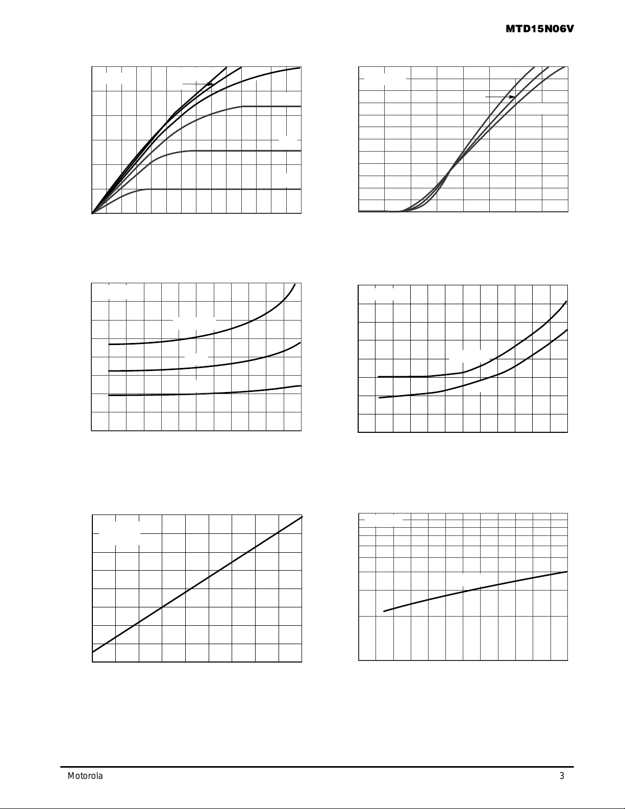
TYPICAL ELECTRICAL CHARACTERISTICS
0 1 2 3 5 7
0
10
20
30
VDS, DRAIN–TO–SOURCE VOLTAGE (VOLTS)
Figure 1. On–Region Characteristics
I
D
, DRAIN CURRENT (AMPS)
2 4 6 8 10
0
5
10
20
30
I
D
, DRAIN CURRENT (AMPS)
VGS, GATE–TO–SOURCE VOLTAGE (VOLTS)
Figure 2. Transfer Characteristics
0 5 10 15 20 30
0
0.05
0.10
0.20
R
DS(on)
, DRAIN–TO–SOURCE RESISTANCE (OHMS)
ID, DRAIN CURRENT (AMPS)
Figure 3. On–Resistance versus Drain Current
and Temperature
Figure 4. On–Resistance versus Drain Current
and Gate Voltage
0 10 20 40 50 60
10
100
Figure 5. On–Resistance Variation with
Temperature
VDS, DRAIN–TO–SOURCE VOLTAGE (VOLTS)
Figure 6. Drain–To–Source Leakage
Current versus Voltage
I
DSS
, LEAKAGE (nA)
TJ = 25
°C
VGS = 10 V
9 V
8 V
6 V
5 V
7 V
VGS = 10 V
TJ = 100
°C
25
°C
– 55
°C
TJ = – 55
°C
25
°C
100
°C
VGS = 0 V
TJ = 125
°C
5
15
25
4 6
15
25
25
30
VDS ≥ 10 V
0.15
R
DS(on)
, DRAIN–TO–SOURCE RESISTANCE (OHMS)
ID, DRAIN CURRENT (AMPS)
TJ = 25°C
0.13
0.11
0.09
0.07
0.05
1050 15 20 25 30
VGS = 10 V
15 V
R
DS(on)
, DRAIN–TO–SOURCE RESISTANCE
(NORMALIZED)
TJ, JUNCTION TEMPERATURE (°C)
VGS = 10 V
ID = 7.5 A
2
1.6
1.2
0.8
0.4
–50 –25 0 25 50 75 100 125 150
175
 Loading...