Motorola MRF650 Datasheet

SEMICONDUCTOR TECHNICAL DATA
The RF Line
Designed for 12.5 Volt UHF large–signal amplifier applications in industrial
and commercial FM equipment operating to 520 MHz.
• Guaranteed 440, 470, 512 MHz 12.5 Volt Characteristics
Output Power = 50 Watts
Minimum Gain = 5.2 dB @ 440, 470 MHz
Efficiency = 55% @ 440, 470 MHz
IRL = 10 dB
• Characterized with Series Equivalent Large–Signal Impedance Parameters
from 400 to 520 MHz
• Built–In Matching Network for Broadband Operation
• Triple Ion Implanted for More Consistent Characteristics
• Implanted Emitter Ballast Resistors
• Silicon Nitride Passivated
• 100% Tested for Load Mismatch Stress at all Phase Angles with 20:1
VSWR @ 15.5 Vdc, 2.0 dB Overdrive
• Circuit board photomaster available upon request by contacting
RF Tactical Marketing in Phoenix, AZ.
Order this document
by MRF650/D
50 W, 512 MHz
RF POWER
TRANSISTOR
NPN SILICON
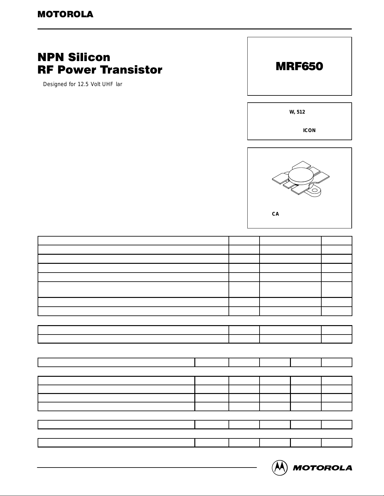
CASE 316–01, STYLE 1
MAXIMUM RATINGS
Rating Symbol Value Unit
Collector–Emitter Voltage V
Collector–Emitter Voltage V
Emitter–Base Voltage V
Collector Current — Continuous I
Total Device Dissipation @ TC = 25°C
Derate above 25°C
Storage Temperature Range T
Operating Junction Temperature T
THERMAL CHARACTERISTICS
Characteristic Symbol Max Unit
Thermal Resistance, Junction to Case R
ELECTRICAL CHARACTERISTICS (T
Characteristic
= 25°C unless otherwise noted)
C
Symbol Min Typ Max Unit
OFF CHARACTERISTICS
Collector–Emitter Breakdown V oltage (IC = 50 mAdc, IB = 0) V
Collector–Emitter Breakdown Voltage (IC = 50 mAdc, VBE = 0) V
Emitter–Base Breakdown Voltage (IE = 10 mAdc, IC = 0) V
Collector Cutoff Current (VCE = 15 Vdc, VBE = 0, TC = 25°C) I
(BR)CEO
(BR)CES
(BR)EBO
CES
ON CHARACTERISTICS
DC Current Gain (IC = 1.0 Adc, VCE = 5.0 Vdc) h
FE
DYNAMIC CHARACTERISTICS
Output Capacitance (VCB = 12.5 Vdc, IE = 0, f = 1.0 MHz) C
REV 8
ob
CEO
CES
EBO
C
P
D
stg
J
θJC
16.5 — — Vdc
38 — — Vdc
4.0 — — Vdc
— — 5.0 mAdc
20 70 120 —
— 135 170 pF
16.5 Vdc
38 Vdc
4.0 Vdc
12 Adc
135
0.77
–65 to +150 °C
200 °C
1.3 °C/W
Watts
W/°C
(continued)
Motorola, Inc. 1997
MRF650MOTOROLA RF DEVICE DATA
1

ELECTRICAL CHARACTERISTICS — continued (T
Characteristic Symbol Min Typ Max Unit
= 25°C unless otherwise noted)
C
FUNCTIONAL TESTS (In Motorola Test Fixture. See Figure 1.)
Common–Emitter Amplifier Power Gain
(VCC = 12.5 Vdc, P
Common–Emitter Amplifier Power Gain
(VCC = 12.5 Vdc, P
Input Return Loss
(VCC = 12.5 Vdc, P
Collector Efficiency
(VCC = 12.5 Vdc, P
Collector Efficiency
(VCC = 12.5 Vdc, P
Output Mismatch Stress
(VCC = 15.5 V, 2.0 dB Overdrive, f = 470 MHz,
VSWR = 20:1, All Phase Angles) (1)
NOTES:
1. Pin = 2.0 dB above drive requirement for 50 W output at 12.5 Vdc.
2. ψ = Mismatch stress factor — the electrical criterion established to verify the device resistance to load mismatch failure. The mismatch stress
test is accomplished in the standard test fixture (Figure 1) terminated in a 20:1 minimum load mismatch at all phase angles.
= 50 W, f = 440, 470 MHz)
out
= 50 W, f = 512 MHz)
out
= 50 W, f = 440, 470, 512 MHz)
out
= 50 W, f = 440, 470 MHz)
out
= 50 W, f = 512 MHz)
out
G
pe
G
pe
IRL 10 15 — dB
η 55 65 — %
— 50 60 — %
ψ (2)
5.2 6.1 — dB
5.0 5.9 — dB
No Degradation in Output Power
R1
∆
V
RE
PORT
RF INPUT
50
Ω
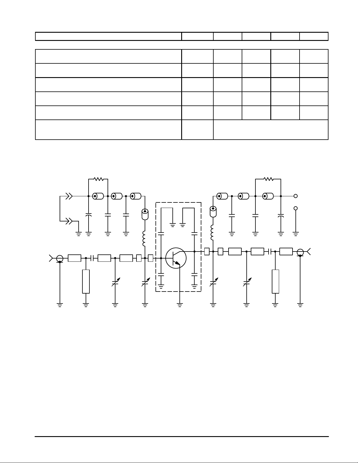
B1, B8 — Ferrite Bead Ferroxcube VK200 20–4B
B2, B3, B4, B5, B6, B7 — Ferrite Bead Ferroxcube #56–590–3B
C1, C8 — 10 µF, 25 V , 25%, Electrolytic, ECS TE–1204
C2, C7 — 1000 pF, Chip Cap, 5%, ATC 100B102JC50
C3, C6 — 91 pF, 5%, Mica, SAHA 3HS0006–91
C4, C5, C12, C13 — 36 pF, 5%, SAHA 3HS0006–36
C9, C16 — 220 pF, Chip Cap, 5%, ATC 100B221JC200
C10, C11, C15 — 0.8–10 pF, Variable, Johanson JMC501 PG26J200
C14 — 1.0–20 pF, Variable, Johanson JMC5501 PG26J200
L1, L2 — 3 Turns, 18 AWG, 0.19″ ID — Total Length 3.5″
N1, N2 — N Coaxial Conn., Omni–Spectra 3052–1648–10
R1, R2 — 10 Ohm, 10%, 1.0 W, Carbon, RCA 831010
TL1
N1
TL2
B1 B2 B3
+
C1 C2 C3 B4
L1
TL3 TL4 TL5 TL6
C9
C10
C11
SOCKET
C4 C5
D.U.T.
C12 C13
Figure 1. 440 to 512 MHz Broadband T est Circuit Schematic
R2
B6 B7 B8
B5
L2
C6 C7
C16
C14 C15
TL1, TL12 — Zo = 50 Ohm
TL2 — See Photomaster
TL3 — See Photomaster
TL4 — See Photomaster
TL5 — See Photomaster
TL6 — See Photomaster
TL7 — See Photomaster
TL8 — See Photomaster
TL9 — See Photomaster
TL10 — See Photomaster
TL11 — See Photomaster
Transmission Line Boards: 1/16″ Glass–Teflon
Transmission Line Boards: Keene GX–0600–55–22
Transmission Line Boards: 2 oz. Cu Clad Both Sides
Transmission Line Boards: εr = 2.55
Bias Boards: 1/16″ G10 or Equivalent
Bias Boards: 2 oz. Cu Clad Double Sided
TL11
C8
+12.5 Vdc
+
TL12TL7 TL8 TL9 TL10
RF
OUTPUT
50
N2
Ω
MRF650
2
MOTOROLA RF DEVICE DATA
 Loading...