

Motorola MRF641 Datasheet
1
MRF641MOTOROLA RF DEVICE DATA
The RF Line
. . . designed for 12.5 Volt UHF large–signal amplifier applications in industrial
and commercial FM equipment operating to 512 MHz.
• Specified 12.5 Volt, 470 MHz Characteristics —
Output Power = 15 Watts
Minimum Gain = 7.8 dB
Efficiency = 55%
• Characterized with Series Equivalent Large–Signal Impedance Parameters
• Built–In Matching Network for Broadband Operation
• Tested for Load Mismatch Stress at all Phase Angles with 20:1 VSWR @
16–Volt High Line and Overdrive
• Circuit board photomaster available upon request by contacting RF Tactical
Marketing in Phoenix, AZ.
MAXIMUM RATINGS
Rating Symbol Value Unit
Collector–Emitter Voltage V
CEO
16 Vdc
Collector–Base Voltage V
CBO
36 Vdc
Emitter–Base Voltage V
EBO
4.0 Vdc
Collector Current — Continuous I
C
3.0 Adc
Total Device Dissipation @ TC = 25°C
Derate above 25°C
P
D
43.7
0.25
Watts
W/°C
Storage Temperature Range T
stg
–65 to +150 °C
THERMAL CHARACTERISTICS
Characteristic Symbol Max Unit
Thermal Resistance, Junction to Case R
θJC
4.0 °C/W
ELECTRICAL CHARACTERISTICS (T
C
= 25°C unless otherwise noted.)
Characteristic
Symbol Min Typ Max Unit
OFF CHARACTERISTICS
Collector–Emitter Breakdown Voltage
(IC = 20 mAdc, IB = 0)
V
(BR)CEO
16 — — Vdc
Collector–Emitter Breakdown Voltage
(IC = 20 mAdc, VBE = 0)
V
(BR)CES
36 — — Vdc
Emitter–Base Breakdown Voltage
(IE = 5.0 mAdc, IC = 0)
V
(BR)EBO
4.0 — — Vdc
Collector Cutoff Current
(VCE = 15 Vdc, VBE = 0, TC = 25°C)
I
CES
— — 5.0 mAdc
(continued)
Order this document
by MRF641/D
SEMICONDUCTOR TECHNICAL DATA
15 W, 470 MHz
CONTROLLED Q
RF POWER
TRANSISTOR
NPN SILICON
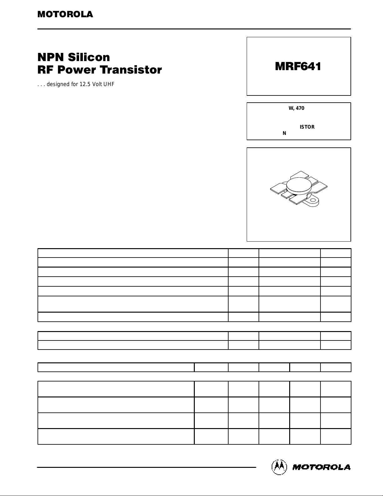
CASE 316–01, STYLE 1
Motorola, Inc. 1994
REV 6
MRF641
2
MOTOROLA RF DEVICE DATA
ELECTRICAL CHARACTERISTICS — continued (T
C
= 25°C unless otherwise noted.)
Characteristic
Symbol Min Typ Max Unit
ON CHARACTERISTICS
DC Current Gain
(IC = 1.0 Adc, VCE = 5.0 Vdc)
h
FE
30 70 150 —
DYNAMIC CHARACTERISTICS
Output Capacitance
(VCB = 12.5 Vdc, IE = 0, f = 1.0 MHz)
C
ob
— 40 60 pF
FUNCTIONAL TESTS
Common–Emitter Amplifier Power Gain
(VCC = 12.5 Vdc, P
out
= 15 W, f = 470 MHz)
G
pe
7.8 8.5 — dB
Collector Efficiency
(VCC = 12.5 Vdc, P
out
= 15 W, f = 470 MHz)
η 55 60 — %
Output Mismatch Stress
(VCC = 16 Vdc, Pin = 3.0 W, f = 470 MHz,
VSWR = 20:1, All Phase Angles)
ψ
No Degradation in Output Power
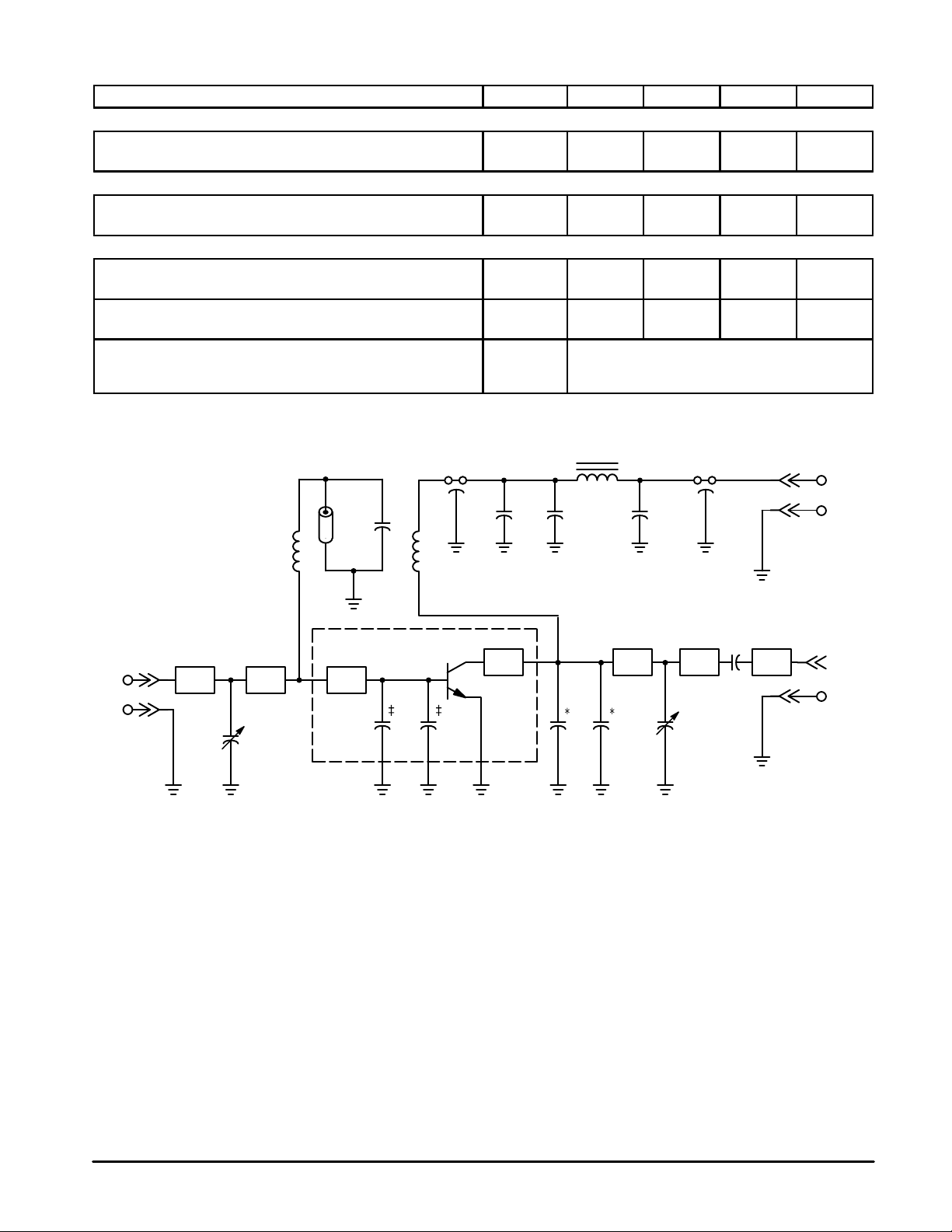
Figure 1. Test Circuit Schematic
Z1 — 1.225″ x 0.187″ Microstrip
Z2 — 0.884″ x 0.187″ Microstrip
Z3 — Capacitor Block (Base)
Z4 — Collector Block
Z5 — 1.1″ x 0.187″ Microstrip
Z6 — 0.433″ x 0.187″ Microstrip
Z7 — 0.4″ x 0.187″ Microstrip
Dotted Area — Capacitor Assembly
C1, C2 — 0.8–10 pF Johanson
C3, C4 — 24 pF Chip Caps 100 mils ATC
C5, C6 — 22 pF Chip Caps 100 mils ATC
C12 — 220 pF Chip Cap 100 mils ATC
C7, C11 — 1.0 µF Tantalum 35 Vdc
C9, C10 — 680 pF Feedthrough Allen–Bradley
C13 — 200 pF UNELCO
C8 — 0.1 µF, 50 V Erie Red Cap
RFC1 — VK 200 — 104B Ferrite Choke
L1 — 4 Turns 0.2″ Dia. #16 AWG
L2 — 9 Turns 0.15″ Dia. #16 AWG
Bead — Ferroxcube 56–590–65–35EB
*C5, C6, are mounted as close to the capacitor
*assembly as possible.
‡‡C3, C4 are mounted in the capacitor assembly.
Board — 62.5 mil Glass Teflon, εr = 2.55.
PARTS NOTES
RF INPUT
RF OUTPUT
BEAD
RFC1
VCC12.5 V
C10C9
+
–
C7 C8 C11
+
–
C13
L2
C1
C3 C4 C5 C6
C2
C12
Z7Z6Z5Z4
Z3Z2Z1
} }
* *
L1
 Loading...