

Motorola MRF6402 Datasheet

SEMICONDUCTOR TECHNICAL DATA
The RF Line
The MRF6402 is designed for 1.8 GHz Personal Communications Network
(PCN) base stations applications. It incorporates high value emitter ballast
resistors, gold metallizations and offers a high degree of reliability and
ruggedness. For ease of design, this transistor has an internally matched input.
• To be used in Class AB for PCN and Cellular Radio Applications
• Specified 26 V, 1.88 GHz Characteristics
Output Power — 4.5 Watts
Gain — 10 dB Typ
Efficiency — 45% Typ
• Circuit board photomaster available upon request by contacting
RF Tactical Marketing in Phoenix, AZ.
Order this document
by MRF6402/D
4.5 W, 1.88 GHz
RF POWER TRANSISTOR
NPN SILICON
CASE 319–07, STYLE 2
MAXIMUM RATINGS
Rating Symbol Value Unit
Collector–Emitter Voltage V
Collector–Base Voltage V
Emitter–Base Voltage V
Collector–Current — Continuous I
Total Device Dissipation @ TC = 25°C
Derate above 25°C
Storage Temperature Range T
Operating Junction Temperature T
CER
CBO
EBO
C
P
D
stg
J
40 Vdc
45 Vdc
3.5 Vdc
0.7 Adc
15
0.2
–65 to +150 °C
200 °C
Watts
W/°C
THERMAL CHARACTERISTICS
Characteristic Symbol Max Unit
Thermal Resistance, Junction to Case (1) R
ELECTRICAL CHARACTERISTICS (T
Characteristic
= 25°C unless otherwise noted.)
C
Symbol Min Typ Max Unit
θJC
5 °C/W
OFF CHARACTERISTICS
Collector–Emitter Breakdown V oltage
(IC = 10 mA, RBE = 75 Ω)
Emitter–Base Breakdown Voltage
(IE = 5 mAdc)
Collector–Base Breakdown Voltage (IC = 10 mAdc) V
Collector–Emitter Leakage (VCE = 26 V, RBE = 75 Ω) I
(1) Thermal resistance is determined under specified RF operating condition. (continued)
V
(BR)CER
V
(BR)EBO
(BR)CBO
CER
40 — — Vdc
3.5 — — Vdc
40 — — Vdc
— — 5 mA
REV 7
Motorola, Inc. 1997
MRF6402MOTOROLA RF DEVICE DATA
1
ELECTRICAL CHARACTERISTICS — continued (T
Characteristic
ON CHARACTERISTICS
DC Current Gain
(IC = 0.1 Adc, VCE = 20 Vdc)
DYNAMIC CHARACTERISTICS
Output Capacitance
(VCB = 26 V, IE = 0, f = 1 MHz)
FUNCTIONAL TESTS
Common–Emitter Amplifier Power Gain
(VCC = 26 V, P
Collector Efficiency
(VCC = 26 V, P
Load Mismatch
(VCC = 26 V, P
Load VSWR = 3:1, All Phase Angles at Frequency of Test)
= 4 W, ICQ = 40 mA, f = 1.88 GHz)
out
= 4 W, f = 1.88 GHz)
out
= 4.5 W, ICQ = 40 mA, f = 1.88 GHz,
out
= 25°C unless otherwise noted.)
C
Symbol Min Typ Max Unit
h
FE
C
ob
G
p
η 40 43 — %
Ψ
50 — 200 —
— 6 — pF
9 10 — dB
No Degradation in Output Power
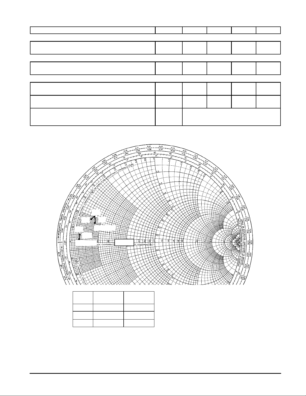
1.84
1.75
1.75
ZOL*
f = 1.95 GHz
f
(GHz)
1.75
1.84
1.95
Z
in
f = 1.95 GHz
Z
in
(Ω)
0.12 + j0.18
0.13 + j0.2
0.15 + j0.16
Zo = 50
Ω
ZOL*
(Ω)
0.06 + j0.05
0.06 + j0.04
0.06 + j0.02
ZOL*: Conjugate of optimum load impedance
into which the device operates at a
given output power, voltage, current
and frequency.
Figure 1. Input and Output Impedances with Circuit T uned for Maximum Gain
@ VCE = 26 V, ICQ = 40 mA, P
out
= 4.5 W
MRF6402
2
MOTOROLA RF DEVICE DATA
 Loading...