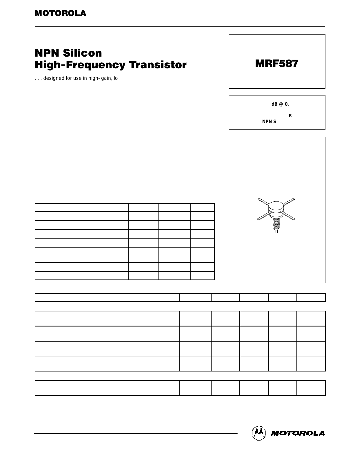
Motorola MRF587 Datasheet

1
MRF587MOTOROLA RF DEVICE DATA
The RF Line
. . . designed for use in high–gain, low–noise, ultra–linear, tuned and wideband
amplifiers. Ideal for use in CATV, MATV, and instrumentation applications.
• Low Noise Figure —
NF = 3.0 dB (Typ) @ f = 500 MHz, IC = 90 mA
• High Power Gain —
G
U(max)
= 16.5 dB (Typ) @ f = 500 MHz
• Ion Implanted
• All Gold Metal System
• High fT — 5.5 GHz
• Low Intermodulation Distortion:
TB3 = –70 dB
DIN = 125 dB µV
• Nichrome Emitter Ballast Resistors
MAXIMUM RATINGS
Rating Symbol Value Unit
Collector–Emitter Voltage V
CEO
17 Vdc
Collector–Base Voltage V
CBO
34 Vdc
Emitter–Base Voltage V
EBO
2.5 Vdc
Collector Current — Continuous I
C
200 mAdc
Total Device Dissipation @ TC = 50°C
Derate above TC = 50°C
P
D
5.0
33
Watts
mW/°C
Storage Temperature Range T
stg
– 65 to +150 °C
Junction Temperature T
J
200 °C
ELECTRICAL CHARACTERISTICS (T
C
= 25°C unless otherwise noted.)
Characteristic
Symbol Min Typ Max Unit
OFF CHARACTERISTICS
Collector–Emitter Breakdown Voltage
(IC = 5.0 mAdc, IB = 0)
V
(BR)CEO
17 — — Vdc
Collector–Base Breakdown Voltage
(IC = 1.0 mAdc, IE = 0)
V
(BR)CBO
34 — — Vdc
Emitter–Base Breakdown Voltage
(IC = 0, IE = 0.1 mAdc)
V
(BR)EBO
2.5 — — Vdc
Collector Cutoff Current
(VCB = 10 Vdc, IE = 0)
I
CBO
— — 50 µAdc
ON CHARACTERISTICS
DC Current Gain (1)
(IC = 50 mAdc, VCE = 5.0 Vdc)
h
FE
50 — 200 —
NOTE: (continued)
1. 300 µs pulse on Tektronix 576 or equivalent.
Order this document
by MRF587/D
SEMICONDUCTOR TECHNICAL DATA
NF = 3.0 dB @ 0.5 GHz
HIGH–FREQUENCY
TRANSISTOR
NPN SILICON
CASE 244A–01, STYLE 1
Motorola, Inc. 1994
REV 6

MRF587
2
MOTOROLA RF DEVICE DATA
ELECTRICAL CHARACTERISTICS — continued (T
C
= 25°C unless otherwise noted.)
Characteristic
Symbol Min Typ Max Unit
DYNAMIC CHARACTERISTICS
Current–Gain — Bandwidth Product (2)
(IC = 90 mAdc, VCE = 15 Vdc, f = 0.5 GHz)
f
T
— 5.5 — GHz
Collector–Base Capacitance
(VCB = 10 Vdc, IE = 0, f = 1.0 MHz)
C
cb
— 1.7 2.2 pF
FUNCTIONAL TESTS
Narrowband — Figure 15
(IC = 90 mA, VCC = 15 V, f = 0.5 GHz)
Noise Figure
Power Gain at Optimum Noise Figure
NF
G
NF
—
11
3.0
13
4.0
—
dB
Broadband — Figure 16
(IC = 90 mA, VCC = 15 V, f = 0.3 GHz)
Noise Figure
Power Gain at Optimum Noise Figure
NF
G
NF
—
—
6.3
11
—
—
dB
Triple Beat Distortion
(IC = 50 mA, VCC = 15 V, P
Ref
= 50 dBmV)
(IC = 90 mA, VCC = 15 V, P
Ref
= 50 dBmV)
TB
3
— –70 — dB
DIN 45004
(IC = 90 mA, VCC = 15 V)
(IC = 90 mA, VCC = 15 V)
DIN — 125 — dBµV
Maximum Available Power Gain (3)
(IC = 90 mA, VCE = 15 Vdc, f = 0.5 GHz)
G
Umax
— 16.5 — dB
NOTES:
2. Characterized on HP8542 Automatic Network Analyzer
3. G
Umax
=
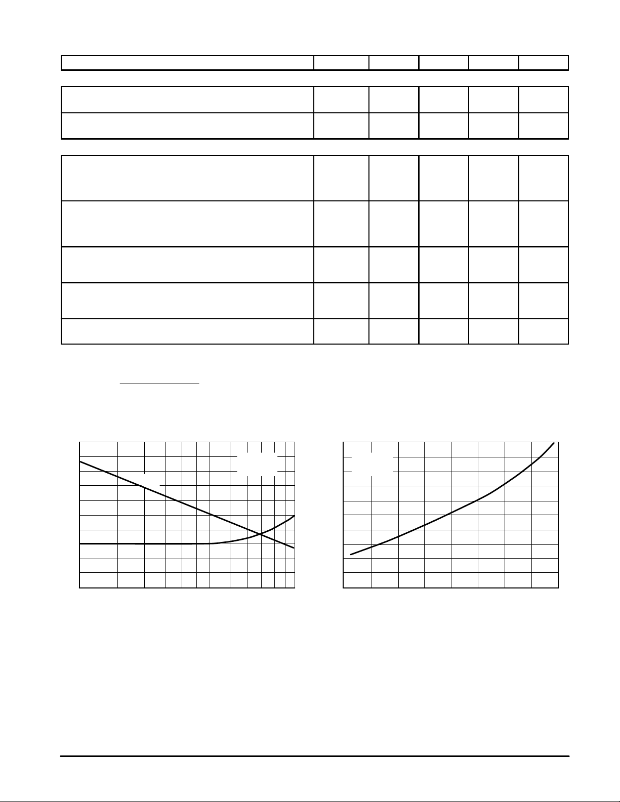
Figure 1. Typical Noise Figure and
Associated Gain versus Frequency
Figure 2. Noise Figure versus Collector Current
10
0.20.1
f, FREQUENCY (GHz)
0.3 0.5 0.7 10
G
NF
, GAIN AT NOISE FIGURE (dB)
NF, NOISE FIGURE (dB)
3
0
G
NF
VCE = 15 V
IC = 90 mA
9
8
7
6
5
4
3
2
1
0
0.9
6
9
12
15
18
21
24
27
30
500
IC, COLLECTOR CURRENT (mA)
NF, NOISE FIGURE (dB)
6
5
4
3
2
1
100 150 200
VCE = 15 V
f = 300 MHz
N.F.
|S
21
|
2
(1
–
|S11|2)(1–|S
22
|2)

3
MRF587MOTOROLA RF DEVICE DATA
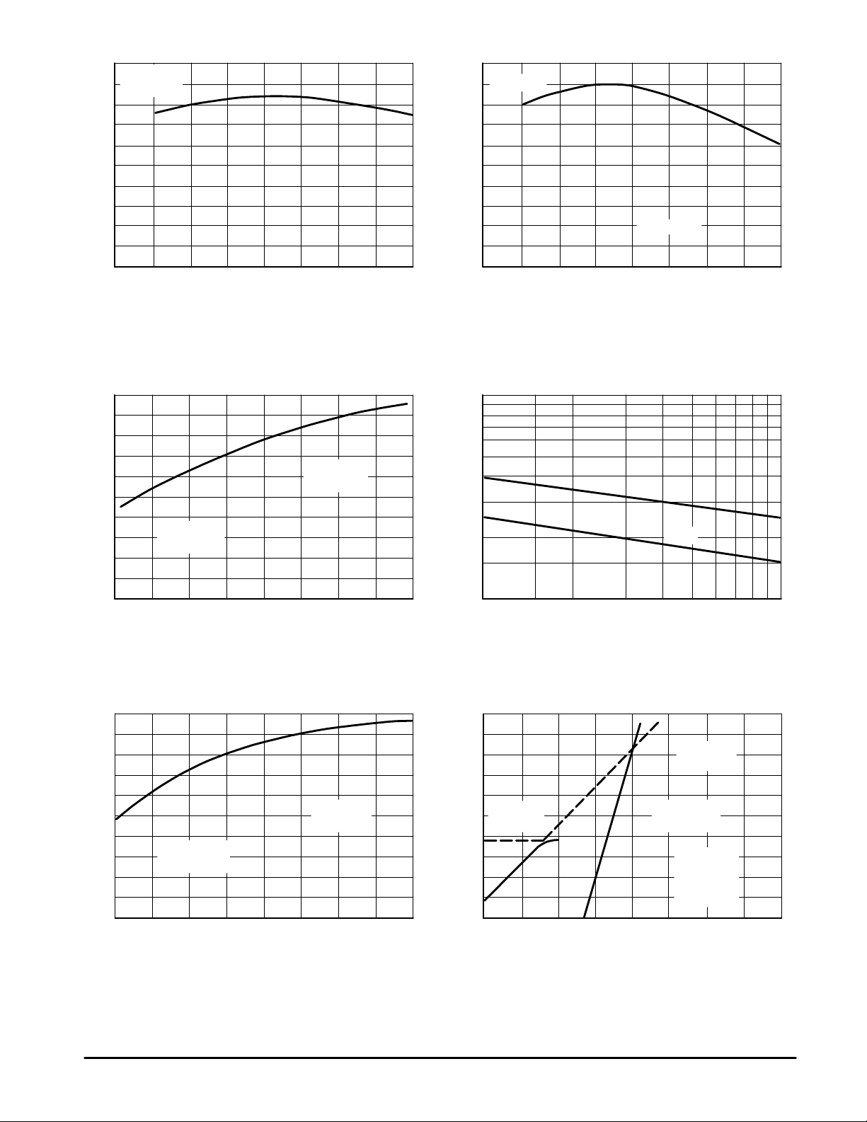
Figure 3. G
Umax
versus Collector Current Figure 4. Gain–Bandwidth Product versus
Collector Current
f , GAIN-BANDWIDTH PRODUCT (GHz)
T
500
IC, COLLECTOR CURRENT (mA)
6
5
4
3
2
1
100 150 200500
IC, COLLECTOR CURRENT (mA)
20
100 150 200
16
12
8
4
0
G
Umax
, MAXIMUM AVAILABLE POWER GAIN (dB)
f = 500 MHz
VCE = 15 V
VCE = 15 V
f = 1000 MHz
Figure 5. Broadband Noise Figure Figure 6. Junction Capacitance versus Voltage
Figure 7. 1.0 dB Compression Point versus
Collector Current
Figure 8. Third Order Intercept Point
TYPICAL PERFORMANCE
NF, NOISE FIGURE (dB)
7
6
5
4
3
2
VCC = 15 V
f = 300 MHz
CIRCUIT PER
FIGURE 16
1009080
70605040
IC, COLLECTOR CURRENT (mA)
110 120
VCB, COLLECTOR BASE VOLTAGE (V)
CAPACITANCE (pF)
10
1 2
7
5
3
2
1
3 5 7 10
C
ob
C
cb
V
out
, OUTPUT VOLTAGE (dBmV)
80
76
72
68
64
60
1009080
70605040
IC, COLLECTOR CURRENT (mA)
110 120
VCC = 15 V
f = 200 MHz
CIRCUIT PER
FIGURE 16
P , OUTPUT POWER (dBm)
out
P , OUTPUT POWER (dBm)
out
31
29
27
25
23
21
19
17
15
13
11
60
80
706050403020
Pin, INPUT POWER (dBm)
50
40
30
20
10
100
3RD ORDER
INTERCEPT
f1 = 205 MHz
f2 = 211 MHz
VCC = 15 V
IC = 90 mA
+1 dB
COMP. PT.
CIRCUIT PER
FIGURE 16
 Loading...