

Motorola MRF555 Datasheet

1
MRF555MOTOROLA RF DEVICE DATA
The RF Line
Designed primarily for wideband large signal predriver stages in the UHF
frequency range.
• Specified @ 12.5 V, 470 MHz Characteristics @ P
out
= 1.5 W
Common Emitter Power Gain = 12.5 dB (Typ)
Efficiency 60% (Typ)
• Cost Effective PowerMacro Package
• Electroless Tin Plated Leads for Improved Solderability
• Circuit board photomaster available upon request by
contacting RF Tactical Marketing in Phoenix, AZ.
MAXIMUM RATINGS
Rating Symbol Value Unit
Collector–Emitter Voltage V
CEO
16 Vdc
Collector–Base Voltage V
CBO
36 Vdc
Emitter–Base Voltage V
EBO
4.0 Vdc
Collector Current — Continuous I
C
400 mAdc
Operating Junction Temperature T
J
150 °C
Total Device Dissipation @ TC = 75°C (1, 2)
Derate above 75°C
P
D
3.0
40
Watts
mW/°C
Storage Temperature Range T
stg
–55 to +150 °C
THERMAL CHARACTERISTICS
Characteristic Symbol Max Unit
Thermal Resistance, Junction to Case R
θJC
25 °C/W
ELECTRICAL CHARACTERISTICS (T
A
= 25°C unless otherwise noted)
Characteristic Symbol Min Typ Max Unit
OFF CHARACTERISTICS
Collector–Emitter Breakdown Voltage
(IC = 5.0 mAdc, IB = 0)
V
(BR)CEO
16 — — Vdc
Collector–Emitter Breakdown Voltage
(IC = 5.0 mAdc, VBE = 0)
V
(BR)CES
36 — — Vdc
Emitter–Base Breakdown Voltage
(IE = 0.1 mAdc, IC = 0)
V
(BR)EBO
4.0 — — Vdc
Collector Cutoff Current
(VCE = 15 Vdc, VBE = 0, TC = 25°C)
I
CES
— — 0.1 mAdc
ON CHARACTERISTICS
DC Current Gain
(IC = 100 mAdc, VCE = 5.0 Vdc)
h
FE
50 90 200 —
DYNAMIC CHARACTERISTICS
Output Capacitance
(VCB = 15 Vdc, IE = 0, f = 1.0 MHz)
C
ob
— 3.5 5.0 pF
NOTES: (continued)
1. TC, Case temperature measured on collector lead immediately adjacent to body of package.
2. The MRF555 PowerMacro must be properly mounted for reliable operation. AN938, “Mounting Techniques in PowerMacro Transistor,”
discusses methods of mounting and heatsinking.
Order this document
by MRF555/D
SEMICONDUCTOR TECHNICAL DATA
1.5 W, 470 MHz
RF LOW POWER
TRANSISTOR
NPN SILICON
CASE 317D–02, STYLE 2
Motorola, Inc. 1995
REV 7
MRF555
2
MOTOROLA RF DEVICE DATA
ELECTRICAL CHARACTERISTICS — continued (T
A
= 25°C unless otherwise noted)
Characteristic
Symbol Min Typ Max Unit
FUNCTIONAL TESTS (f = 470 MHz)
Common–Emitter Power Gain
(VCC = 12.5 Vdc, P
out
= 1.5 W)
G
pe
11 12.5 — dB
Collector Efficiency
(VCC = 12.5 Vdc, P
out
= 1.5 W)
η
c
50 60 — %
Load Mismatch Stress
(VCC = 15.5 Vdc, Pin = 125 mW,
VSWR ≥ 10:1 all phase angles)
ψ
No Degradation in Output Power
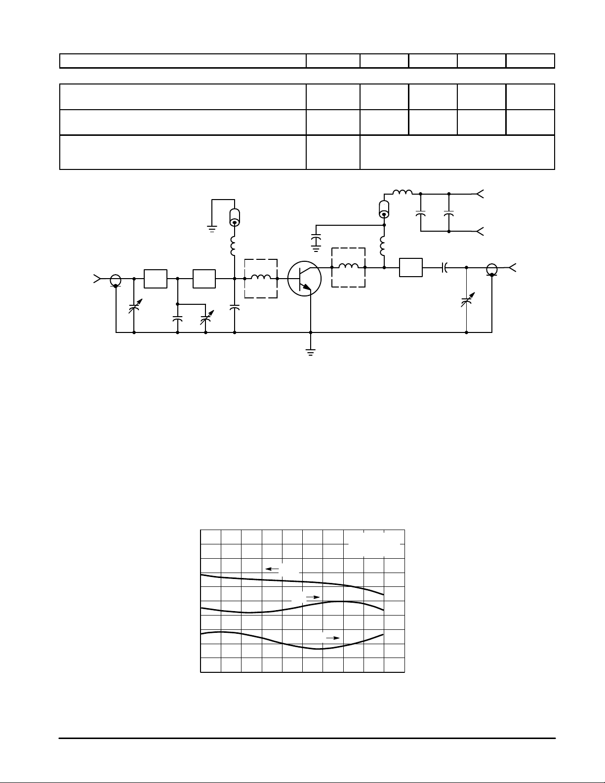
Figure 1. 400–512 MHz Broadband Circuit
*C1, C3, C6 — 0.8–11 pF Johanson
C2 — 15 pF Clamped Mica, Mini–Underwood
C4 — 36 pF Clamped Mica, Mini–Underwood
C5 — 470 pF Ceramic Chip Capacitor
C7 — 91 pF Clamped Mica, Mini–Underwood
C8 — 68 pF Clamped Mica, Mini–Underwood
C9 — 1.0 µF, 25 V Tantalum
B — Bead, Ferroxcube 56–590–65/3B
*Fixed tuned for broadband response
L1 — 5 Turns #21 AWG, 5/32″ I.D.
L2, L3 — 60 x 125 x 250 Mils Copper Pad on 27 Mil Thick
L2, L3 — Alumina Substrate
L4, L5 — 7 Turns #21 AWG 5/32″ I.D.
Z1 — 1.29″ x 0.16″ Microstrip
Z2 — 0.70″ x 0.16″ Microstrip
Z3 — 2.18″ x 0.16″ Microstrip
PCB — 1/16″ Glass Teflon, 1 oz. cu. clad,
PCB — double sided, εr = 2.5
Figure 2. Performance in Broadband Circuit
RF
POWER
INPUT
RF
POWER
OUTPUT
B
D.U.T.
Z1 Z2
Z3
C1
C2
C3
C4
L2
L3
C7
L4
B
L5
C8 C9
+
+
–
C5
C6
G
pe
, POWER GAIN (dB)
c
η
, COLLECTOR
20
16
12
8
0
4
400
65
60
f, FREQUENCY (MHz)
425 450 475 500 525
20
15
10
55
EFFICIENCY
%
IRL, INPUT
RETURN LOSS
(dB)
G
pe
η
c
IRL
P
out
= 1.5 W
VCC = 12.5 Vdc
V
CC
L1
 Loading...