

Motorola MRF5003 Datasheet
1
MRF5003MOTOROLA RF DEVICE DATA
The RF MOSFET Line
N–Channel Enhancement–Mode
The MRF5003 is designed for broadband commercial and i ndustrial
applications at frequencies to 520 MHz. The high gain and b roadband
performance of this device makes it ideal for large–signal, common source
amplifier applications in 7.5 Volt and 12.5 Volt mobile, portable, and base
station FM equipment.
• Guaranteed Performance at 512 MHz, 7.5 Volts
Output Power = 3.0 Watts
Power Gain = 9.5 dB
Efficiency = 45%
• Characterized with Series Equivalent Large–Signal Impedance Parameters
• S–Parameter Characterization at High Bias Levels
• Excellent Thermal Stability
• All Gold Metal for Ultra Reliability
• Capable of Handling 20:1 VSWR, @ 15.5 Vdc, 512 MHz, 2.0 dB Overdrive
• Suitable for 12.5 Volt Applications
• True Surface Mount Package
• Available in Tape and Reel by Adding R1 Suffix to Part Number.
R1 Suffix = 500 Units per 16 mm, 7 inch Reel.
• Circuit board photomaster available upon request by contacting
RF Tactical Marketing in Phoenix, AZ.
MAXIMUM RATINGS
Rating Symbol Value Unit
Drain–Source Voltage V
DSS
36 Vdc
Drain–Gate Voltage (RGS = 1.0 Meg Ohm) V
DGR
36 Vdc
Gate–Source Voltage V
GS
±20 Vdc
Drain Current — Continuous I
D
1.7 Adc
Total Device Dissipation @ TC = 25°C
Derate above 25°C
P
D
12.5
0.07
Watts
W/°C
Storage Temperature Range T
stg
–65 to +150 °C
Operating Junction Temperature T
J
200 °C
THERMAL CHARACTERISTICS
Characteristic Symbol Max Unit
Thermal Resistance, Junction to Case R
θJC
14 °C/W
NOTE – CAUTION – MOS devices are susceptible to damage from electrostatic charge. Reasonable precautions in handling and
packaging MOS devices should be observed.
Order this document
by MRF5003/D
SEMICONDUCTOR TECHNICAL DATA
3.0 W, 7.5 V, 512 MHz
N–CHANNEL
BROADBAND
RF POWER FET
CASE 430–01, STYLE 2
Motorola, Inc. 1994
REV 6

MRF5003
2
MOTOROLA RF DEVICE DATA
ELECTRICAL CHARACTERISTICS (T
C
= 25°C unless otherwise noted.)
Characteristic
Symbol Min Typ Max Unit
OFF CHARACTERISTICS
Drain–Source Breakdown Voltage
(VGS = 0, ID = 2.5 mAdc)
V
(BR)DSS
36 — — Vdc
Zero Gate Voltage Drain Current
(VDS = 15 Vdc, VGS = 0)
I
DSS
— — 1.0 mAdc
Gate–Source Leakage Current
(VGS = 20 Vdc, VDS = 0)
I
GSS
— — 1.0 µAdc
ON CHARACTERISTICS
Gate Threshold Voltage
(VDS = 10 Vdc, ID = 5.0 mAdc)
V
GS(th)
1.25 2.25 3.5 Vdc
Drain–Source On–Voltage
(VGS = 10 Vdc, ID = 0.5 Adc)
V
DS(on)
— — 0.375 Vdc
Forward Transconductance
(VDS = 10 Vdc, ID = 0.5 Adc)
g
fs
0.6 — — mho
DYNAMIC CHARACTERISTICS
Input Capacitance
(VDS = 12.5 Vdc, VGS = 0, f = 1.0 MHz)
C
iss
— 16.5 — pF
Output Capacitance
(VDS = 12.5 Vdc, VGS = 0, f = 1.0 MHz)
C
oss
— 37 — pF
Reverse Transfer Capacitance
(VDS = 12.5 Vdc, VGS = 0, f = 1.0 MHz)
C
rss
3.5 4.4 5.4 pF
FUNCTIONAL TESTS (In Motorola Test Fixture)
Common–Source Amplifier Power Gain
(VDD = 7.5 Vdc, P
out
= 3.0 W, IDQ = 50 mA) f = 512 MHz
f = 175 MHz
G
ps
9.5
—
10.5
15
—
—
dB
Drain Efficiency
(VDD = 7.5 Vdc, P
out
= 3.0 W, IDQ = 50 mA) f = 512 MHz
f = 175 MHz
h
45
—
50
55
—
—
%
3
MRF5003MOTOROLA RF DEVICE DATA
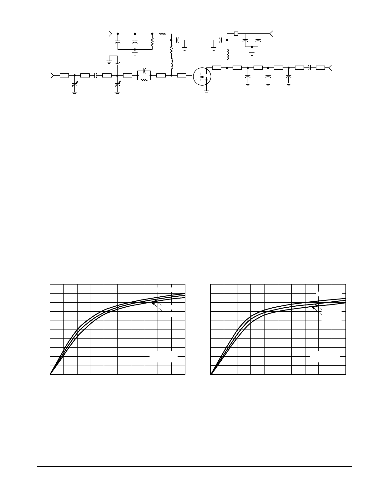
10
8
6
4
2
0
0 100 200 300 400 500
f = 400 MHz
470 MHz
520 MHz
VDD = 12.5 V
IDQ = 50 mA
Pin, INPUT POWER (MILLIWATTS)
P
out
, OUTPUT POWER (WATTS)
5
4
3
2
1
0
0 100 200 300 400 500
f = 400 MHz
470 MHz
520 MHz
VDD = 7.5 V
IDQ = 50 mA
Pin, INPUT POWER (MILLIWATTS)
P
out
, OUTPUT POWER (WATTS)
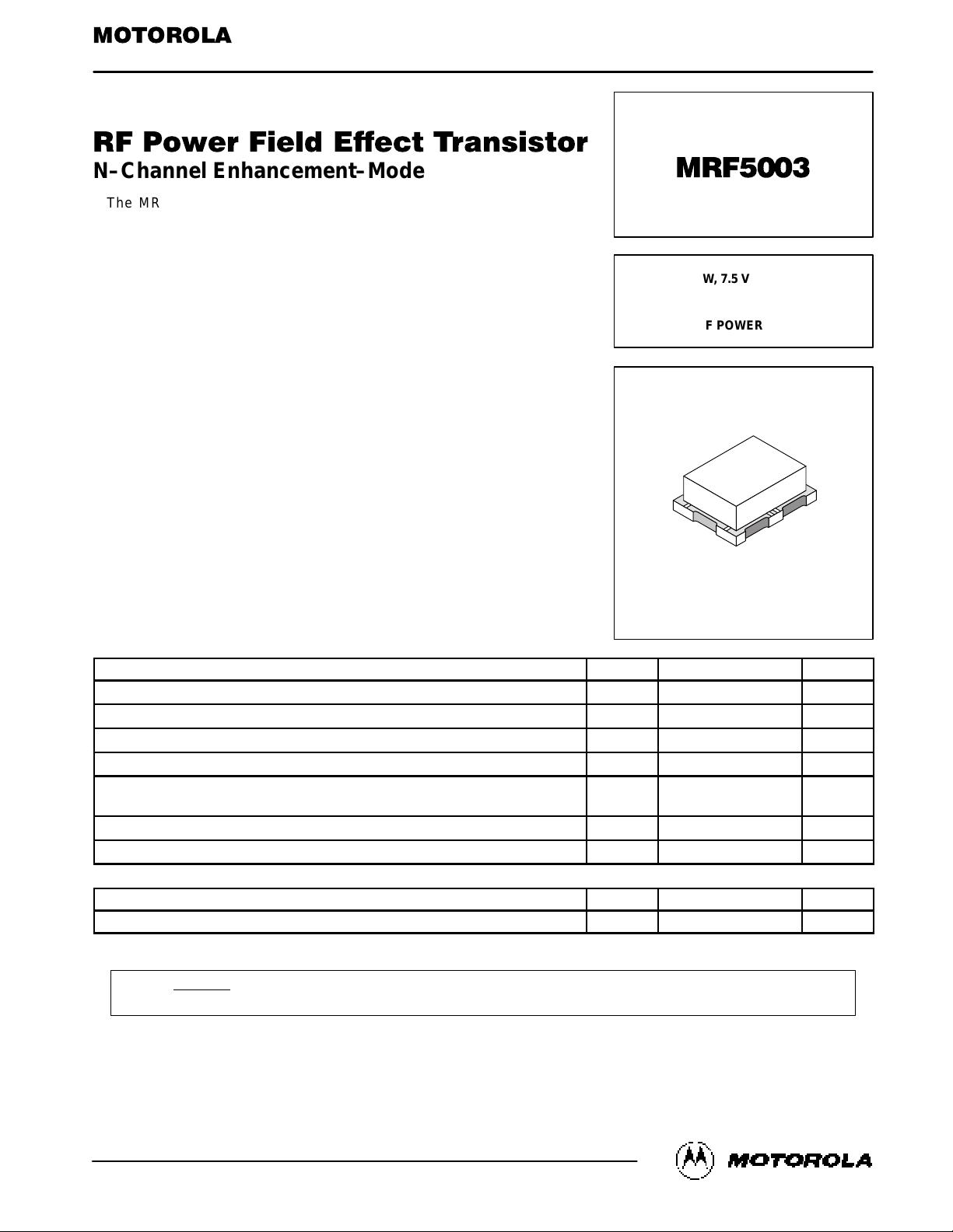
C1, C3, C7, C8 0 to 20 pF Johanson
C2, C9 56 pF, 100 mil Chip
C4 10 pF, 100 mil Chip
C5 47 pF, Miniature Clamped Mica Capacitor
C6 22 pF, 100 mil Chip
C10, C15 10 µF, 50 V, Electrolytic
C11, C14 0.1 µF, Capacitor
C12 1000 pF, 100 mil Chip
C13 160 pF, 100 mil Chip
R1 35 Ω, 1/4 W Carbon
R2 30 Ω, 0.1 W Chip
R3 1.0 kΩ, 0.1 W Chip
R4 1.0 MΩ, 1/4 W Carbon
B1 Fair Rite Products Short Ferrite Bead (2743021446)
Board — Glass Teflon, 31 mils
Note: Plated ceramic part locators (0.1″ x 0.15″) soldered onto Z6 and Z7.
Z1 0.350″ x 0.08″ Microstrip
Z2 0.190″ x 0.08″ Microstrip
Z3 0.800″ x 0.08″ Microstrip
Z4 0.380″ x 0.08″ Microstrip
Z5 0.150″ x 0.08″ Microstrip
Z6 0.285″ x 0.08″ Microstrip
Z7 0.340″ x 0.08″ Microstrip
Z8 0.070″ x 0.08″ Microstrip
Z9 0.280″ x 0.08″ Microstrip
Z10 0.840″ x 0.08″ Microstrip
Z11 0.180″ x 0.08″ Microstrip
Z12 0.600″ x 0.08″ Microstrip
L1 7 Turns, 0.076″ ID, #24 AWG Enamel
L2 5 Turns, 0.126″ ID, #20 AWG Enamel
Input/Output Connectors — Type N
Figure 1. 512 MHz Narrowband Test Circuit
TYPICAL CHARACTERISTICS
Figure 2. Output Power versus Input Power Figure 3. Output Power versus Input Power
V
GG
RF
INPUT
RF
OUTPUT
C10 C11 R4
R3
C12 C13
C14 C15
B1
L2
Z7 Z8 Z9 Z10 Z11 Z12
C6 C7 C8
C9
Z6Z5Z4Z3Z2Z1
C1 C3 R1
C5
R2
V
DD
C2
D.U.T.
L1C4
 Loading...