Motorola MRF464 Datasheet

1
MRF464MOTOROLA RF DEVICE DATA
The RF Line
. . . designed primarily for applications as a high–power linear amplifier from 2.0
to 30 MHz, in single sideband mobile, marine and base station equipment.
• Specified 28 Volt, 30 MHz Characteristics —
Output Power = 80 W (PEP)
Minimum Gain = 15 dB
Efficiency = 40%
Intermodulation Distortion = –32 dB (Max)
MATCHING PROCEDURE
In the push–pull circuit configuration it is preferred that the transistors are
used as matched pairs to obtain optimum performance.
The matching procedure used by Motorola consists of measuring hFE at the
data sheet conditions and color coding the device to predetermined hFE ranges
within the normal hFE limits. A color dot is added to the marking on top of the
cap. Any two devices with the same color dot can be paired together to form a
matched set of units.
MAXIMUM RATINGS
Rating Symbol Value Unit
Collector–Emitter Voltage V
CEO
35 Vdc
Collector–Base Voltage V
CBO
65 Vdc
Emitter–Base Voltage V
EBO
4.0 Vdc
Collector Current — Continuous I
C
10 Adc
Total Device Dissipation @ TC = 25°C
Derate above 25°C
P
D
250
1.4
Watts
W/°C
Storage Temperature Range T
stg
–65 to +150 °C
THERMAL CHARACTERISTICS
Characteristic Symbol Max Unit
Thermal Resistance, Junction to Case R
θJC
0.7 °C/W
Stud Torque (1) — 8.5 In. Lb.
ELECTRICAL CHARACTERISTICS (T
C
= 25°C unless otherwise noted.)
Characteristic
Symbol Min Max Unit
OFF CHARACTERISTICS
Collector–Emitter Breakdown Voltage
(IC = 100 mAdc, IB = 0)
V
(BR)CEO
35 — Vdc
Collector–Emitter Breakdown Voltage
(IC = 100 mAdc, VBE = 0)
V
(BR)CES
65 — Vdc
Emitter–Base Breakdown Voltage
(IE = 1.0 mAdc, IC = 0)
V
(BR)EBO
4.0 — Vdc
Collector Cutoff Current
(VCE = 28 Vdc, VBE = 0, TC = +55°C)
I
CES
— 10 mAdc
ON CHARACTERISTICS
DC Current Gain
(IC = 0.5 Adc, VCE = 5.0 Vdc)
h
FE
10 — —
NOTE: (continued)
1. Case 145A–10 — For Repeated Assembly Use 11 In. Lb.
Order this document
by MRF464/D
SEMICONDUCTOR TECHNICAL DATA
80 W (PEP), 30 MHz
RF POWER
TRANSISTOR
NPN SILICON
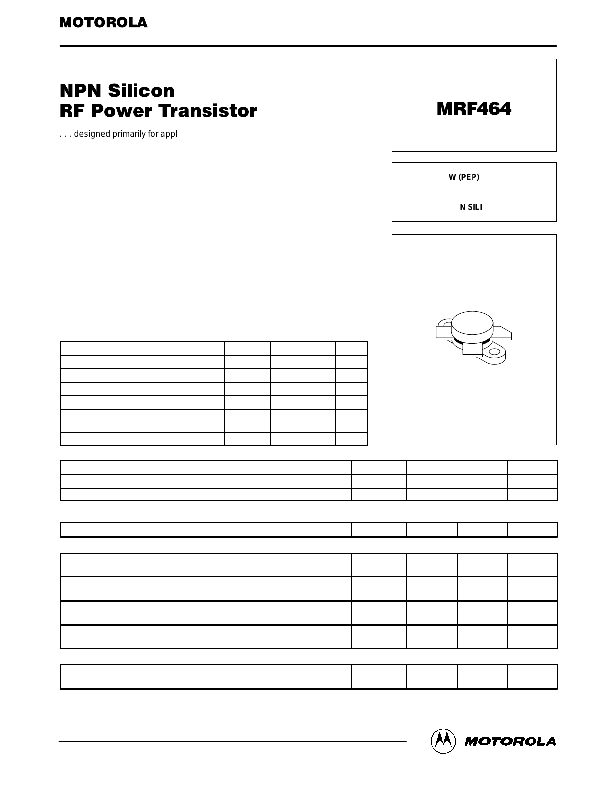
CASE 211–11, STYLE 1
Motorola, Inc. 1994

MRF464
2
MOTOROLA RF DEVICE DATA
ELECTRICAL CHARACTERISTICS — continued (T
C
= 25°C unless otherwise noted.)
Characteristic UnitMaxMinSymbol
DYNAMIC CHARACTERISTICS
Output Capacitance
(VCB = 28 Vdc, IE = 0, f = 1.0 MHz)
C
ob
— 200 pF
FUNCTIONAL TESTS
Common–Emitter Amplifier Power Gain (Figure 1)
(P
out
= 80 W (PEP), IC = 3.6 Adc (Max), VCC = 28 Vdc,
f1 = 30 MHz, f2 = 30.001 MHz)
G
PE
15 — dB
Intermodulation Distortion Ratio (Figure 1) (2)
(P
out
= 80 W (PEP), IC = 3.6 Adc (Max), VCC = 28 Vdc,
f1 = 30 MHz, f2 = 30.001 MHz)
IMD — –32 dB
Collector Efficiency
(P
out
= 80 W (PEP), IC = 3.6 Adc (Max), VCC = 28 Vdc,
f1 = 30 MHz, f2 = 30.001 MHz)
η 40 — %
NOTE:
2. To Mil–Std–1311 Version A, Test Method 2204B, Two Tone, Reference each Tone.
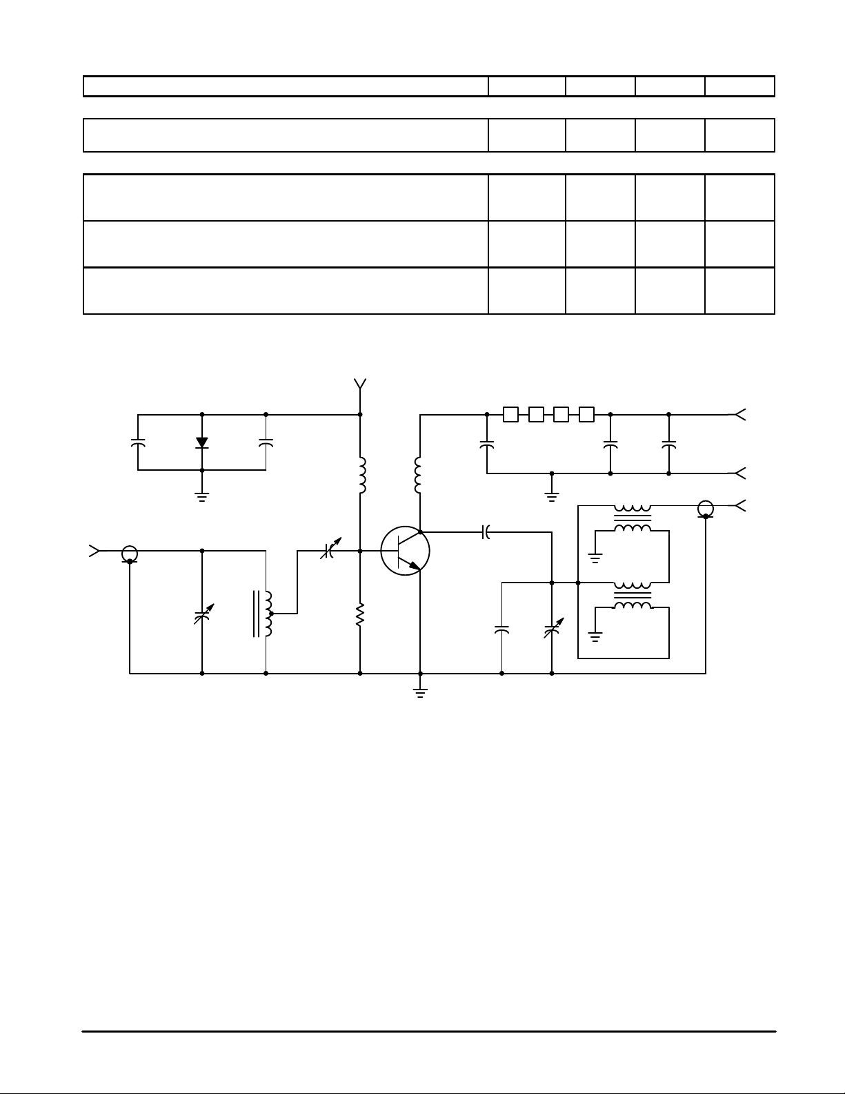
Figure 1. 30 MHz Test Circuit
RF BEADS
C1C2
DUT
–
+
28 Vdc
RL = 50
Ω
RFC
2000 pF
BUTTON
0.01
µ
F
10
µ
H
RFC
25
µ
F
0.01
µ
F500 µF
ARCO 469
(170–780 pF)
T2
(1:9)
ARCO 466
(80–480 pF)
1N248B
0.1
µ
F
C.T.
T1
10
1/2 W
RFC — 20 Turns @12 AWG Enameled Wire Close Wound in 2 Layers, 1/4″ I.D.
T1 — 20 Turns #24 AWG Wire Wound on Micro–Metals T37–7 Toroid Core
T1 — Center Tapped.
T2 — 1:9 XFMR; 6 Turns of 2 Twisted Pairs of #28 AWG Enameled Wire.
T2 — (8 Crests Per Inch) Bifilar Wound on Each of 2 Separate Balun Cores.
T2 — (Stackpole #57–1503, No. 14 Material) Interconnected as shown
T2 — RF Beads — Ferroxcube #56–590–65/3B
VBB adjusted for ICQ — 40 mAdc (ICQ = Quiescent
VBB adjusted for ICQ — 40 mAdc Collector Current)
C1 — 170–180 pF ARCO 469 or Equivalent
C2 — 330 pF
V
BB
 Loading...