Motorola MRF455 Datasheet

1
MRF455MOTOROLA RF DEVICE DATA
The RF Line
. . . designed for power amplifier applications in industrial, commercial and
amateur radio equipment to 30 MHz.
• Specified 12.5 Volt, 30 MHz Characteristics —
Output Power = 60 Watts
Minimum Gain = 13 dB
Efficiency = 55%
MATCHING PROCEDURE
In the push–pull circuit configuration it is preferred that the transistors are
used as matched pairs to obtain optimum performance.
The matching procedure used by Motorola consists of measuring hFE at the
data sheet conditions and color coding the device to predetermined hFE ranges
within t he normal hFE limits. A color dot is added t o the marking on t op of the c ap.
Any two devices w ith the same color dot can be paired together to form a
matched set of units.
MAXIMUM RATINGS
Rating Symbol Value Unit
Collector–Emitter Voltage V
CEO
18 Vdc
Collector–Emitter Voltage V
CES
36 Vdc
Emitter–Base Voltage V
EBO
4.0 Vdc
Collector Current — Continuous I
C
15 Adc
Total Device Dissipation @ TC = 25°C
Derate above 25°C
P
D
175
1.0
Watts
W/°C
Storage Temperature Range T
stg
–65 to +150 °C
THERMAL CHARACTERISTICS
Characteristic Symbol Max Unit
Thermal Resistance, Junction to Case R
θJC
1.0 °C/W
ELECTRICAL CHARACTERISTICS (T
C
= 25°C unless otherwise noted.)
Characteristic
Symbol Min Typ Max Unit
OFF CHARACTERISTICS
Collector–Emitter Breakdown Voltage
(IC = 100 mAdc, IB = 0)
V
(BR)CEO
18 — — Vdc
Collector–Emitter Breakdown Voltage
(IC = 50 mAdc, VBE = 0)
V
(BR)CES
36 — — Vdc
Emitter–Base Breakdown Voltage
(IE = 10 mAdc, IC = 0)
V
(BR)EBO
4.0 — — Vdc
ON CHARACTERISTICS
DC Current Gain
(IC = 5.0 Adc, VCE = 5.0 Vdc)
h
FE
10 — 150 —
DYNAMIC CHARACTERISTICS
Output Capacitance
(VCB = 12.5 Vdc, IE = 0, f = 1.0 MHz)
C
ob
— — 250 pF
(continued)
Order this document
by MRF455/D
SEMICONDUCTOR TECHNICAL DATA
60 W, 30 MHz
RF POWER
TRANSISTOR
NPN SILICON
CASE 211–07, STYLE 1
Motorola, Inc. 1994

MRF455
2
MOTOROLA RF DEVICE DATA
ELECTRICAL CHARACTERISTICS — continued (T
C
= 25°C unless otherwise noted.)
Characteristic UnitMaxTypMinSymbol
FUNCTIONAL TESTS (Figure 1)
Common–Emitter Amplifier Power Gain
(VCC = 12.5 Vdc, P
out
= 60 W, f = 30 MHz)
G
pe
13 — — dB
Collector Efficiency
(VCC = 12.5 Vdc, P
out
= 60 W, f = 30 MHz)
η 55 — — %
Series Equivalent Input Impedance
(VCC = 12.5 Vdc, P
out
= 60 W, f = 30 MHz)
Z
in
— 1.66–j.844 — Ohms
Series Equivalent Output Impedance
(VCC = 12.5 Vdc, P
out
= 60 W, f = 30 MHz)
Z
out
— 1.73–j.188 — Ohms
Parallel Equivalent Input Impedance
(VCC = 12.5 Vdc, P
out
= 60 W, f = 30 MHz)
Z
in
— 2.09/1030 — Ω/pF
Parallel Equivalent Output Impedance
(VCC = 12.5 Vdc, P
out
= 60 W, f = 30 MHz)
Z
out
— 1.75/330 — Ω/pF
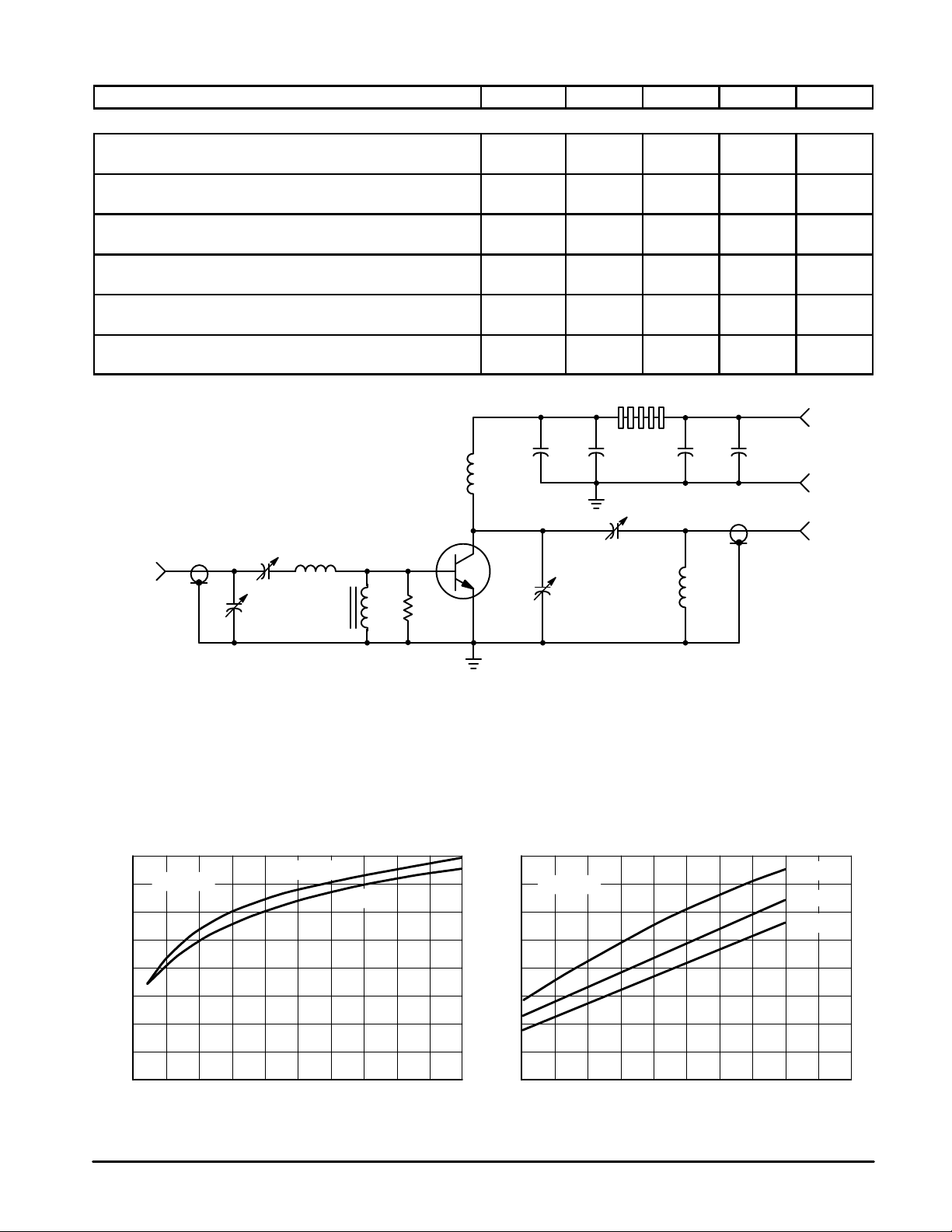
Figure 1. 30 MHz Test Circuit Schematic
f = 30 MHz
P , OUTPUT POWER (WATTS)
out
80
Pin, INPUT POWER (WATTS)
0
70
60
50
40
0
1 2 3 4
5
30
20
10
P , OUTPUT POWER (WATTS)
out
VCC, SUPPLY VOLTAGE (VOLTS)
0.5 1.5 2.5 3.5
4.5
VCC = 13.6 V
80
70
60
50
40
30
20
10
f = 30 MHz
12.5 V
Pin = 3.5 V
1 W
1.75 W
8 10 12 14 16
18
9 11 13 15
17
L3
R1
C5 C6 C7 C8
RF OUTPUT
L4
C4
C1
C2 L2
DUT
C3
L1
–
+
12.5 Vdc
L5
RF INPUT
C1, C2, C4 — ARCO 469
C3 — ARCO 466
C5 — 1000 pF, UNELCO
C6, C7 — 0.1 µF Disc Ceramic
C8 — 1000 µF/15 V Electrolytic
R1 — 10 Ohm/1.0 Watt, Carbon
L1 — 3 Turns, #18 AWG, 5/16″ I.D., 5/16″ Long
L2 — VK200–20/4B, FERROXCUBE
L3 — 12 Turns, #18 AWG Enameled Wire, 1/4″ I.D., Close Wound
L4 — 3 Turns 1/8″ O.D. Copper Tubing, 3/8″ I.D., 3/4″ Long
L5 — 7 FERRITE Beads, FERROXCUBE #56–590–65/3B
90
Figure 2. Output Power versus Input Power Figure 3. Output Power versus Supply Voltage
 Loading...