Motorola MRF448 Datasheet

1
MRF448MOTOROLA RF DEVICE DATA
The RF Line
Designed primarily for high–voltage applications as a high–power linear
amplifier from 2.0 to 30 MHz. Ideal for marine and base station equipment.
• Specified 50 Volt, 30 MHz Characteristics
Output Power = 250 W
Minimum Gain = 12 dB
Efficiency = 45%
• Intermodulation Distortion @ 250 W (PEP) —
IMD = –30 dB (Max)
• 100% Tested for Load Mismatch at all Phase Angles with 3:1 VSWR
MAXIMUM RATINGS
Rating Symbol Value Unit
Collector–Emitter Voltage V
CEO
50 Vdc
Collector–Base Voltage V
CBO
100 Vdc
Emitter–Base Voltage V
EBO
4.0 Vdc
Collector Current — Continuous I
C
16 Adc
Withstand Current — 10 s — 20 Adc
Total Device Dissipation @ TC = 25°C (1)
Derate above 25°C
P
D
290
1.67
Watts
W/°C
Storage Temperature Range T
stg
–65 to +150 °C
THERMAL CHARACTERISTICS
Characteristic Symbol Max Unit
Thermal Resistance, Junction to Case R
θJC
0.6 °C/W
ELECTRICAL CHARACTERISTICS (T
C
= 25°C unless otherwise noted.)
Characteristic
Symbol Min Typ Max Unit
OFF CHARACTERISTICS
Collector–Emitter Breakdown Voltage (IC = 200 mAdc, IB = 0) V
(BR)CEO
50 — — Vdc
Collector–Emitter Breakdown Voltage (IC = 100 mAdc, VBE = 0) V
(BR)CES
100 — — Vdc
Collector–Base Breakdown Voltage (IC = 100 mAdc, IE = 0) V
(BR)CBO
100 — — Vdc
Emitter–Base Breakdown Voltage (IE = 10 mAdc, IC = 0) V
(BR)EBO
4.0 — — Vdc
NOTE: (continued)
1. PD is a measurement reflecting short term maximum condition. See SOAR curve for operating conditions.
Order this document
by MRF448/D
SEMICONDUCTOR TECHNICAL DATA
250 W, 30 MHz
RF POWER
TRANSISTOR
NPN SILICON
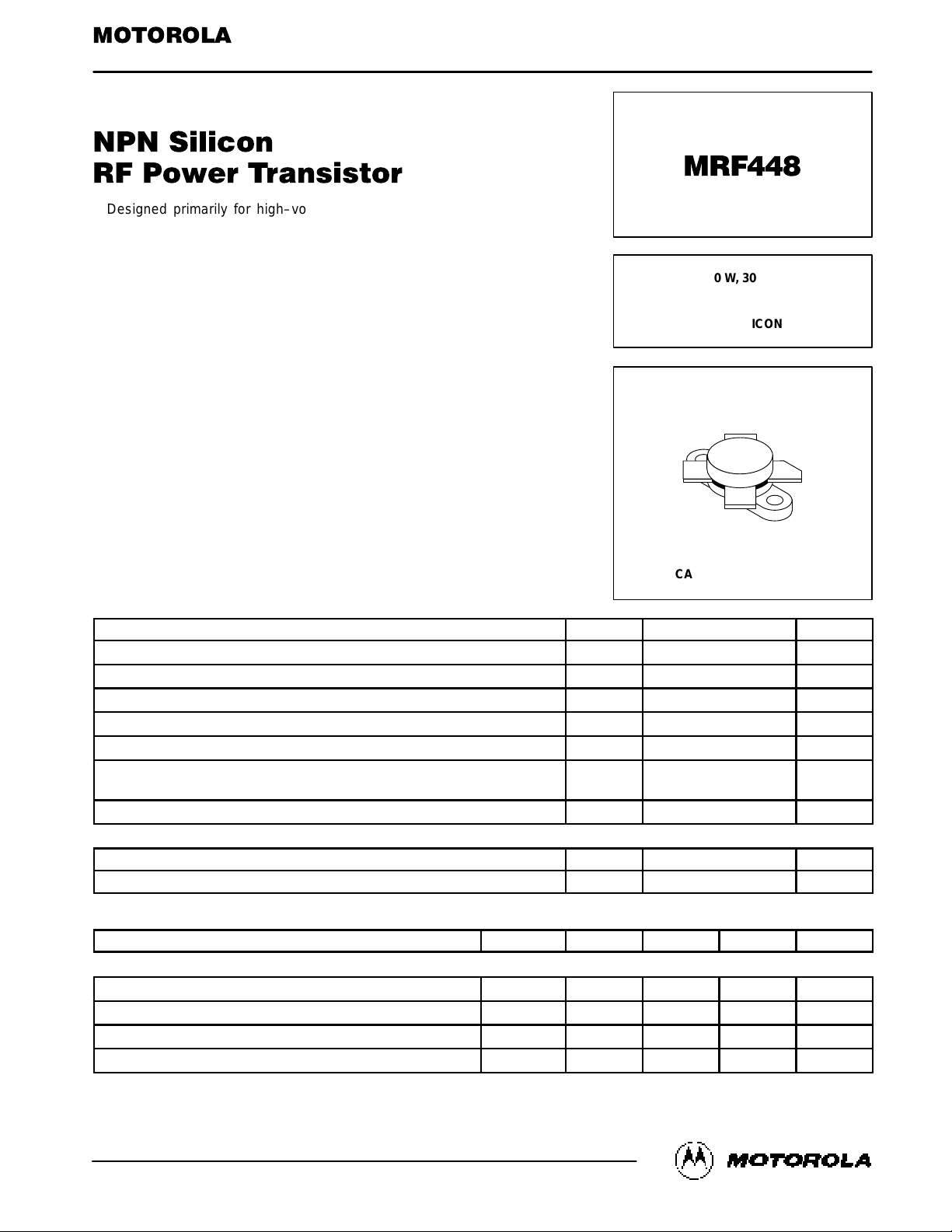
CASE 211–11, STYLE 1
Motorola, Inc. 1994

MRF448
2
MOTOROLA RF DEVICE DATA
ELECTRICAL CHARACTERISTICS — continued (T
C
= 25°C unless otherwise noted.)
Characteristic UnitMaxTypMinSymbol
ON CHARACTERISTICS
DC Current Gain
(IC = 5.0 Adc, VCE = 10 Vdc)
h
FE
10 30 — —
DYNAMIC CHARACTERISTICS
Output Capacitance
(VCB = 50 Vdc, IE = 0, f = 1.0 MHz)
C
ob
— 350 450 pF
FUNCTIONAL TESTS
Common–Emitter Amplifier Power Gain
(VCC = 50 Vdc, P
out
= 250 W CW, f = 30 MHz, ICQ = 250 mA)
G
PE
12 14 — dB
Collector Efficiency
(VCC = 50 Vdc, P
out
= 250 W, f = 30 MHz, ICQ = 250 mA)
η —
—
45
65
—
—
% (PEP)
% (CW)
Intermodulation Distortion (2)
(VCE = 50 Vdc, P
out
= 250 W (PEP), ICQ = 250 mA, f = 30 MHz)
IMD — –33 –30 dB
Electrical Ruggedness
(VCC = 50 Vdc, P
out
= 250 W CW, f = 30 MHz,
VSWR 3:1 at all Phase Angles)
ψ
No Degradation in Output Power
NOTE:
2. To Mil–Std–1311 Version A, Test Method 2204, Two Tone, Reference each Tone.
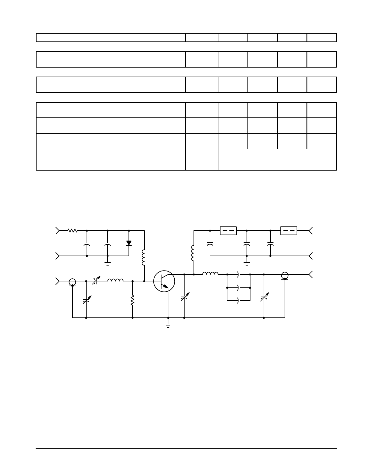
Figure 1. 30 MHz Test Circuit Schematic
C1, C2, C5, C7 — 170–780 pF, Arco 469
C3, C8, C9 — 0.1 µF, 100 V Erie
C4 — 500 µF @ 6.0 V
C6 — 360 pF, 3 x 120 pF 3.0 kV in parallel
C10 — 10 µF, 100 V
R1 — 10 Ω, 10 Watt
R2 — 10 Ω, 1.0 Watt
CR1 — 1N4997 or equivalent
L1 — 3 Turns, #16 Wire, 0.4″ I.D., 0.3″ Long
L2 — 0.8 µH, Ohmite Z–235 or equivalent
L3 — 12 Turns, #16 Enameled Wire Closewound 0.25″ I.D.
L4 — 4 Turns, 1/8″ Copper Tubing, 0.6″ I.D., 1.0″ Long
L5, L6 — 2.0 µH, Fair–Rite 2643021801 Ferrite bead each or equivalent
BIAS
+
RF
INPUT
RF
OUTPUT
50 Vdc
+
–
R1
C3 C4
+
–
CR1
C1
C2
L1
R2
L2
D.U.T.
L3
C5
L4
C8 C9 C10
+
–
L5 L6
C6
C7
 Loading...