Motorola MRF4427R2 Datasheet

SEMICONDUCTOR TECHNICAL DATA
The RF Line
Designed for amplifier, frequency multiplier, or oscillator applications in
industrial equipment constructed with surface mount components. Suitable for
use as output driver or pre–driver stages in VHF and UHF equipment.
• Low Cost SORF Plastic Surface Mount Package
• Guaranteed RF Specification — |S21|
• S–Parameter Characterization
• Low Voltage Version of MRF3866
• Tape and Reel Packaging Available.
R2 suffix = 2,500 units per reel
2
Order this document
by MRF4427/D
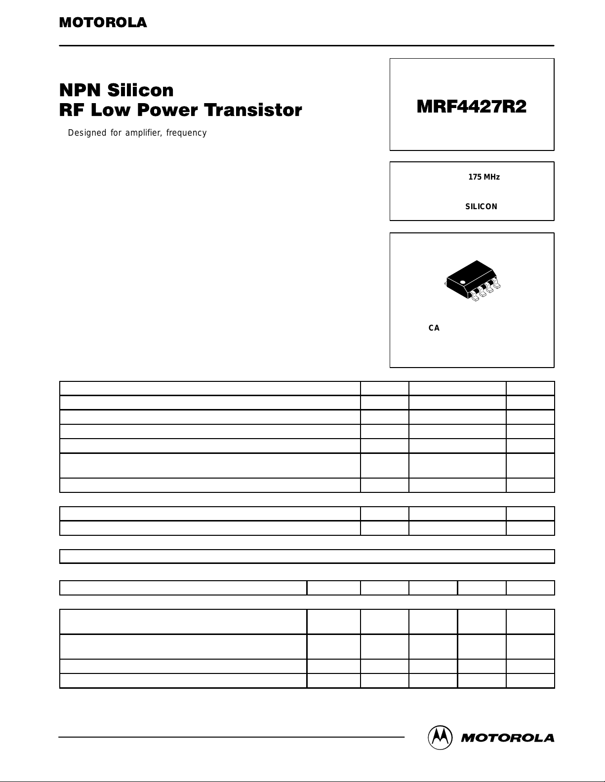
1.0 W, 175 MHz
HIGH–FREQUENCY
TRANSISTOR
NPN SILICON
CASE 751–05, STYLE 1
SORF
(SO–8)
MAXIMUM RATINGS
Rating Symbol Value Unit
Collector–Emitter Voltage V
Collector–Base Voltage V
Emitter–Base Voltage V
Collector Current — Continuous I
Total Device Dissipation @ TC = 75°C
Derate above 75°C
Operating Junction and Storage Temperature Range TJ, T
CEO
CBO
EBO
P
C
D
stg
20 Vdc
40 Vdc
2.0 Vdc
400 mAdc
1.67
22.2
–65 to +150 °C
Watts
mW/°C
THERMAL CHARACTERISTICS
Characteristic Symbol Max Unit
Thermal Resistance, Junction to Case R
θJC
45 °C/W
DEVICE MARKING
MRF4427 = 4427
ELECTRICAL CHARACTERISTICS (T
Characteristic
= 25°C unless otherwise noted)
A
Symbol Min Typ Max Unit
OFF CHARACTERISTICS
Collector–Emitter Sustaining V oltage
(IC = 5.0 mAdc, IB = 0)
Collector–Emitter Breakdown Voltage
(IC = 5.0 mAdc, RBE = 10 ohms)
Emitter–Base Breakdown Voltage (IE = 100 µAdc) V
Collector Cutoff Current (VCE = 12 Vdc, IB = 0) I
NOTE: (continued)
1.Case temperature measured on collector lead immediately adjacent to body of package.
V
(BR)CEO
V
(BR)CER
(BR)EBO
CEO
20 — — Vdc
40 — — Vdc
2.0 — — Vdc
— — 20 µAdc
REV 8
Motorola, Inc. 1997
MRF4427R2MOTOROLA RF DEVICE DATA
1

ELECTRICAL CHARACTERISTICS — continued (T
Characteristic
ON CHARACTERISTICS
DC Current Gain
(IC = 100 mAdc, VCE = 5.0 Vdc)
(IC = 360 mAdc, VCE = 5.0 Vdc)
Collector–Emitter Saturation Voltage
(IC = 100 mAdc, IB = 20 mAdc)
DYNAMIC CHARACTERISTICS
Current–Gain — Bandwidth Product
(IC = 50 mAdc, VCE = 12 Vdc, f = 200 MHz)
Output Capacitance
(VCB = 12 Vdc, IE = 0, f = 1.0 MHz)
FUNCTIONAL TESTS
Common–Emitter Amplifier Power Gain
(Pin = 15 mW, VCC = 12 Vdc, f = 175 MHz)
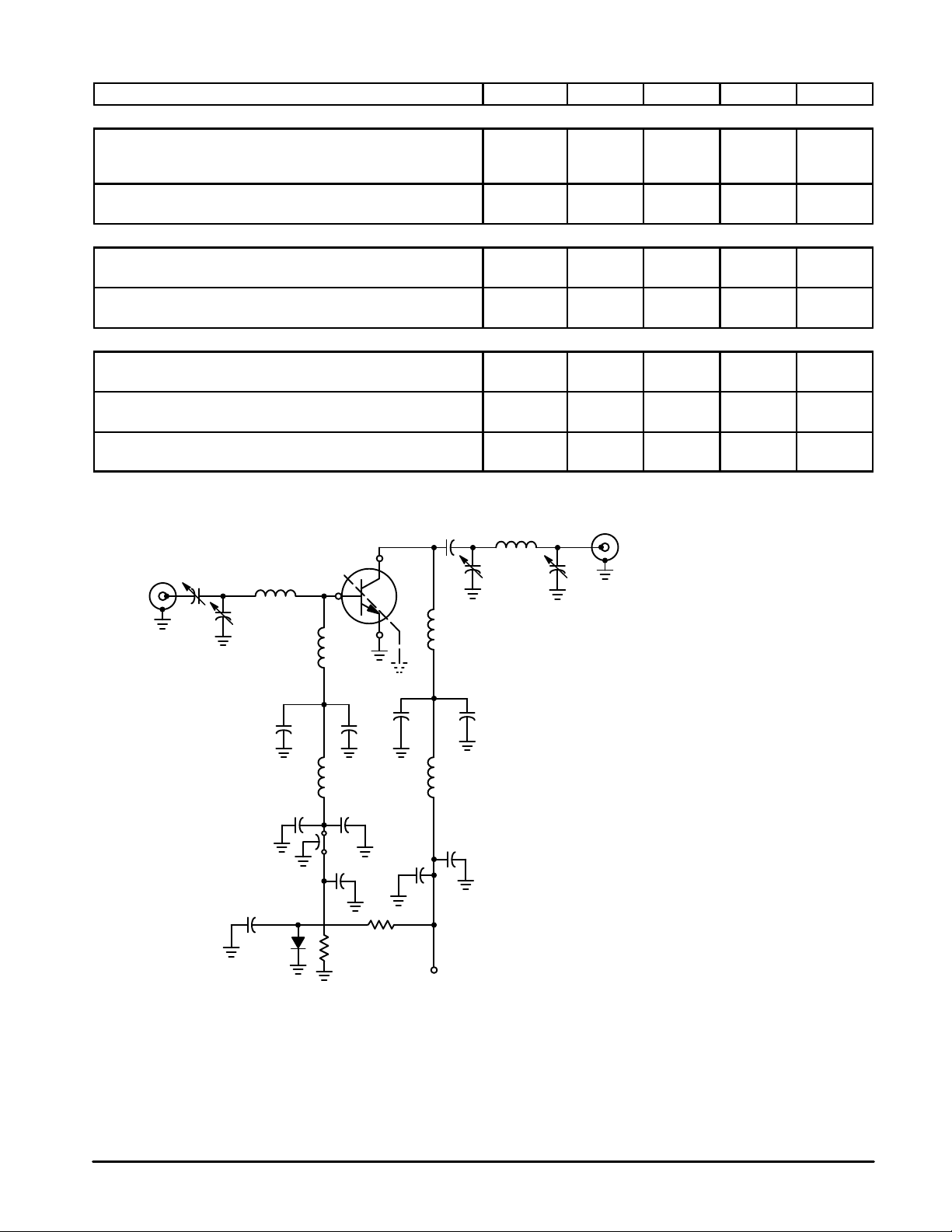
Collector Efficiency (Figure 1)
(P
= 1.0 W, VCC = 12 Vdc, f = 175 MHz)
out
Insertion Gain
(VCE = 12 Vdc, IC = 50 mA, f = 200 MHz)
= 25°C unless otherwise noted)
A
Symbol Min Typ Max Unit
h
FE
V
CE(sat)
f
T
C
ob
G
pe
η — 60 — %
2
|S21|
10
5.0
— 60 — mVdc
— 1600 — MHz
— — 3.0 pF
— 18 — dB
14 16.4 — dB
50
—
200
—
—
C1
C2
C16
L1
RFC1
C10 C11
+
D1
D.U.T.
C6 C7
RFC3
C12
C13
R2
R1
C3 L2
RFC2
C8 C9
RFC4
C15
C14
V
CC
C4 C5
C1, C2 — 5.5–18 pF Erie ceramic trimmer
C3 — 1000 pF ATC 100 mil chip cap.
C4 — 9.0–35 pF Erie ceramic trimmer
C5 — Arco 405 mica trimmer
C6, C8, C10, C14 — 0.1 µF Erie blue cap.
C7, C9 — 470 pF ATC 100 mil chip cap.
C11, C13, C15 — 1.0 µF Erie blue cap, non–polar
C12 — 1000 pF feedthru
C16 — 10 µF, 25 V tantalum
D1 — 1N4148 or 1N914
L1 — 6T #20 AWG on #2 drill bit
L2 — 4T #20 AWG on #4 drill bit
R1 — 4.7 kΩ 1/8 watt carbon
R2 — 100 Ω 1/8 watt carbon
RFC1–4 — 10 µH molded choke
MRF4427R2
2
Figure 1. 175 MHz RF Amplifier Circuit for Functional Tests
MOTOROLA RF DEVICE DATA
 Loading...