

Motorola MRF393 Datasheet
SEMICONDUCTOR TECHNICAL DATA
The RF Line
. . . designed primarily for wideband large–signal output and driver amplifier
stages in the 30 to 500 MHz frequency range.
• Specified 28 Volt, 500 MHz Characteristics —
Output Power = 100 W
Typical Gain = 9.5 dB (Class AB); 8.5 dB (Class C)
Efficiency = 55% (Typ)
• Built–In Input Impedance Matching Networks for Broadband Operation
• Push–Pull Configuration Reduces Even Numbered Harmonics
• Gold Metallization System for High Reliability
• 100% Tested for Load Mismatch
• Circuit board photomaster available upon request by
contacting RF Tactical Marketing in Phoenix, AZ.
2
6
5, 8
1, 4
Order this document
by MRF393/D
100 W, 30 to 500 MHz
CONTROLLED “Q”
BROADBAND PUSH–PULL
RF POWER TRANSISTOR
NPN SILICON
7
3
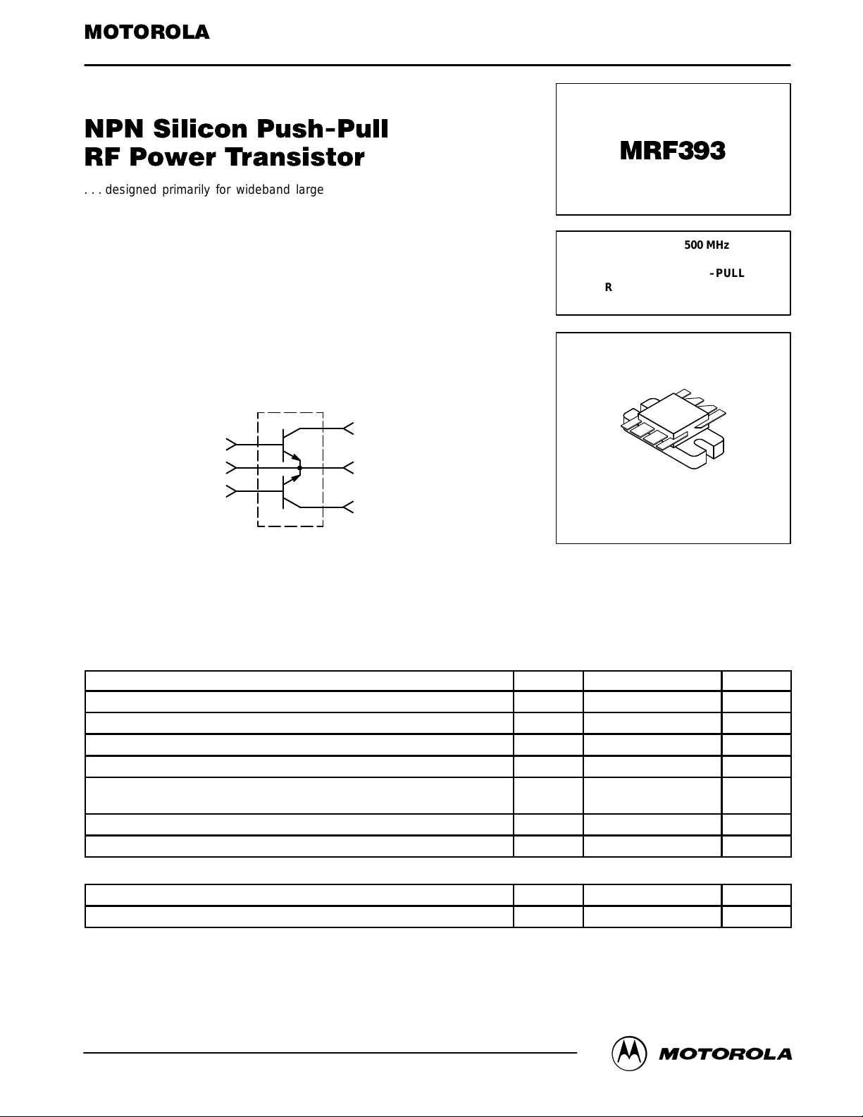
The MRF393 is two transistors in a single package with separate base and collector leads
and emitters common. This arrangement provides the designer with a space saving
device capable of operation in a push–pull configuration.
CASE 744A–01, STYLE 1
PUSH–PULL TRANSISTORS
MAXIMUM RATINGS
Rating Symbol Value Unit
Collector–Emitter Voltage V
Collector–Base Voltage V
Emitter–Base Voltage V
Collector Current — Continuous I
Total Device Dissipation @ TC = 25°C (1)
Derate above 25°C
Storage Temperature Range T
Junction Temperature T
CEO
CBO
EBO
C
P
D
stg
J
30 Vdc
60 Vdc
4.0 Vdc
16 Adc
270
1.54
–65 to +150 °C
200 °C
THERMAL CHARACTERISTICS
Characteristic Symbol Max Unit
Thermal Resistance, Junction to Case R
NOTE:
1. This device is designed for RF operation. The total device dissipation rating applies only when the device is operated as an RF push–pull
amplifier.
θJC
0.65 °C/W
Watts
W/°C
REV 7
Motorola, Inc. 1997
MRF393MOTOROLA RF DEVICE DATA
1

ELECTRICAL CHARACTERISTICS (T
Characteristic Symbol Min Typ Max Unit
= 25°C unless otherwise noted.)
C
OFF CHARACTERISTICS (1)
Collector–Emitter Breakdown V oltage (IC = 50 mAdc, IB = 0) V
Collector–Emitter Breakdown Voltage (IC = 50 mAdc, VBE = 0) V
Emitter–Base Breakdown Voltage (IE = 5.0 mAdc, IC = 0) V
Collector Cutoff Current (VCB = 30 Vdc, IE = 0) I
ON CHARACTERISTICS (1)
DC Current Gain (IC = 1.0 Adc, VCE = 5.0 Vdc) h
DYNAMIC CHARACTERISTICS (1)
Output Capacitance (VCB = 28 Vdc, IE = 0, f = 1.0 MHz) C
FUNCTIONAL TESTS (2) — See Figure 1
Common–Emitter Amplifier Power Gain
(VCC = 28 Vdc, P
Collector Efficiency
(VCC = 28 Vdc, P
Load Mismatch
(VCC = 28 Vdc, P
VSWR = 30:1, all phase angles)
NOTES:
1. Each transistor chip measured separately.
2. Both transistor chips operating in push–pull amplifier.
= 100 W, f = 500 MHz)
out
= 100 W, f = 500 MHz)
out
= 100 W, f = 500 MHz,
out
(BR)CEO
(BR)CES
(BR)EBO
CBO
FE
ob
G
pe
η 50 55 — %
ψ
30 — — Vdc
60 — — Vdc
4.0 — — Vdc
— — 5.0 mAdc
20 — 100 —
40 75 95 pF
7.5 8.5 — dB
No Degradation in Output Power
B1
C1
C2
C1, C2, C7, C8 — 240 pF 100 mil Chip Cap
C3 — 15 pF 100 mil Chip Cap
C4 — 24 pF 100 mil Chip Cap
C5 — 33 pF 100 mil Chip Cap
C6 — 12 pF 100 mil Chip Cap
C9, C13 — 1000 pF 100 mil Chip Cap
C10, C14 — 680 pF Feedthru Cap
C11, C15 — 0.1 µF Ceramic Disc Cap
C12, C16 — 50 µF 50 V
L1
Z1
C4C3
Z2
L2
D.U.T.
C15
L5
C12
L6
C16
C10
C9 C11
L3
Z3 Z5
C5
Z4 Z6
L4
L1
,
L2 — 0.15 µH Molded Choke with Ferrite Bead
L3
,
L4 — 2–1/2 Turns #20 AWG 0.200″ ID
L5
,
L6 — 3–1/2 Turns #18 AWG 0.200″ ID
B1, B2 — Balun 50 Ω Semi Rigid Coax, 86 mil OD, 4″ Long
Z1, Z2 — 850 mil Long x 125 mil W. Microstrip
Z3, Z4 — 200 mil Long x 125 mil W. Microstrip
Z5, Z6 — 800 mil Long x 125 mil W. Microstrip
Board Material — 0.0325″ Teflon–Fiberglass, εr = 2.56,
Board Material — 1 oz. Copper Clad both sides.
C7
C6
C8
C13
B2
C14
+ 28 V
MRF393
2
Figure 1. 500 MHz T est Fixture
MOTOROLA RF DEVICE DATA
 Loading...