

Motorola MRF326 Datasheet
1
MRF326MOTOROLA RF DEVICE DATA
The RF Line
. . . designed primarily for wideband large–signal output amplifier stages in the
100 to 500 MHz frequency range.
• Guaranteed Performance @ 400 MHz, 28 Vdc
Output Power = 40 Watts
Minimum Gain = 9.0 dB
• Built–In Matching Network for Broadband Operation
• 100% Tested for Load Mismatch at all Phase Angles with 30:1 VSWR
• Gold Metallization System for High Reliability Applications
MAXIMUM RATINGS
Rating Symbol Value Unit
Collector–Emitter Voltage V
CEO
33 Vdc
Collector–Base Voltage V
CBO
60 Vdc
Emitter–Base Voltage V
EBO
4.0 Vdc
Collector Current — Continuous
Collector Current — Peak
I
C
4.5
6.0
Adc
Total Device Dissipation @ TC = 25°C (1)
Derate above 25°C
P
D
110
0.63
Watts
W/°C
Storage Temperature Range T
stg
–65 to +150 °C
THERMAL CHARACTERISTICS
Characteristic Symbol Max Unit
Thermal Resistance, Junction to Case R
θJC
1.6 °C/W
ELECTRICAL CHARACTERISTICS (T
C
= 25°C unless otherwise noted.)
Characteristic
Symbol Min Typ Max Unit
OFF CHARACTERISTICS
Collector–Emitter Breakdown Voltage
(IC = 40 mAdc, IB = 0)
V
(BR)CEO
33 — — Vdc
Collector–Emitter Breakdown Voltage
(IC = 40 mAdc, VBE = 0)
V
(BR)CES
60 — — Vdc
Emitter–Base Breakdown Voltage
(IE = 4.0 mAdc, IC = 0)
V
(BR)EBO
4.0 — — Vdc
Collector–Base Breakdown Voltage
(IC = 40 mAdc, IE = 0)
V
(BR)CBO
60 — — Vdc
Collector Cutoff Current
(VCB = 30 Vdc, IE = 0)
I
CBO
— — 4.0 mAdc
ON CHARACTERISTICS
DC Current Gain
(IC = 2.0 Adc, VCE = 5.0 Vdc)
h
FE
20 50 80 —
DYNAMIC CHARACTERISTICS
Output Capacitance
(VCB = 28 Vdc, IE = 0, f = 1.0 MHz)
C
ob
— 45 60 pF
NOTE: (continued)
1. This device is designed for RF operation. The total device dissipation rating applies only when the device is operated as an RF amplifier.
Order this document
by MRF326/D
SEMICONDUCTOR TECHNICAL DATA
40 W, 225 to 400 MHz
CONTROLLED “Q”
BROADBAND RF POWER
TRANSISTOR
NPN SILICON
CASE 316–01, STYLE 1
Motorola, Inc. 1994
MRF326
2
MOTOROLA RF DEVICE DATA
ELECTRICAL CHARACTERISTICS — continued (T
C
= 25°C unless otherwise noted.)
Characteristic UnitMaxTypMinSymbol
FUNCTIONAL TESTS (Figure 1)
Common–Emitter Amplifier Power Gain
(VCC = 28 Vdc, P
out
= 40 W, f = 400 MHz, IC Max = 2.85 Adc)
G
PE
9.0 11 — dB
Collector Efficiency
(VCC = 28 Vdc, P
out
= 40 W, f = 400 MHz, IC Max = 2.85 Adc)
η 50 — — %
Load Mismatch
(VCC = 28 Vdc, P
out
= 40 W CW, f = 400 MHz,
VSWR = 30:1 All Phase Angles)
ψ
No Degradation in Output Power
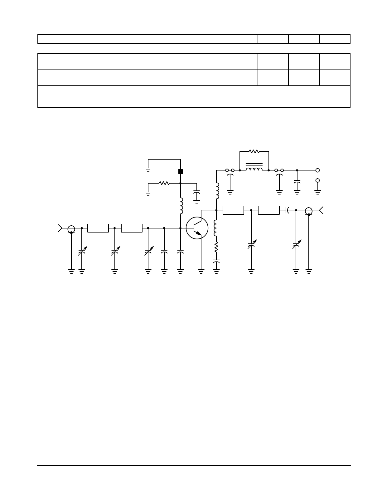
Figure 1. 400 MHz Test Amplifier
C1 — 1.0–10 pF Johanson, Capacitor (JMC 5201)
C2, C3, C6, C8 — 1.0–20 pF Johanson Capacitor
C4, C5 — 36 pF ATC “B” Style Chip Capacitor
C7, C9, C13 — 100 pF UNELCO Capacitor
C11 — 680 pF Feedthru
C10 — 1.0 µF 50 V Tantalum
C12 — 0.1 µF Erie Redcap
L1 — 8 Turns #26 AWG Enameled, 1/16″ ID Closewound
L2, L5 — Ferroxcube VK200–19/4B Ferrite Choke
L3 — 8 Turns #20 AWG Enameled, 1/4″ ID Closewound
L4 — 4 Turns #26 AWG 0.1″ ID
R1 — 10 Ohm 2.0 W Carbon
R2, R3 — 10 Ohm 1.0 W Carbon
Z1 — Microstrip 0.19″ W x 1.28″ L
Z2 — Microstrip 0.28″ W x 1.0″ L
Z3 — Microstrip 0.31″ W x 1.0″ L
Z4 — Microstrip 0.31″ W x 0.9″ L
Board — Glass Teflon εr = 2.56 t = 0.062″
Input/Output Connectors — Type N UG58 A/U
RF
INPUT
RF
OUTPUT
Z1
C1
+
–
28 Vdc
+
Z2
Z3 Z4
C2
C3
C4
C5
DUT
L3
L2
R3
L1
C13
C9
R1
C11
C10
C7
C8
C6
L4
R2
C12
L5
 Loading...