

Motorola MPSA18 Datasheet
1
Motorola Small–Signal Transistors, FETs and Diodes Device Data
NPN Silicon
MAXIMUM RATINGS
Rating Symbol Value Unit
Collector–Emitter Voltage V
CEO
45 Vdc
Collector–Base Voltage V
CBO
45 Vdc
Emitter–Base Voltage V
EBO
6.5 Vdc
Collector Current — Continuous I
C
200 mAdc
Total Device Dissipation @ TA = 25°C
Derate above 25°C
P
D
625
5.0
mW
mW/°C
Total Device Dissipation @ TC = 25°C
Derate above 25°C
P
D
1.5
12
Watts
mW/°C
Operating and Storage Junction
Temperature Range
TJ, T
stg
–55 to +150 °C
THERMAL CHARACTERISTICS
Characteristic Symbol Max Unit
Thermal Resistance, Junction to Ambient R
q
JA
(1)
200 °C/W
Thermal Resistance, Junction to Case R
q
JC
83.3 °C/W
ELECTRICAL CHARACTERISTICS (T
A
= 25°C unless otherwise noted)
Characteristic
Symbol Min Typ Max Unit
OFF CHARACTERISTICS
Collector–Emitter Breakdown Voltage
(2)
(IC = 10 mAdc, IB = 0)
V
(BR)CEO
45 — — Vdc
Collector–Base Breakdown Voltage
(IC = 100 mAdc, IE = 0)
V
(BR)CBO
45 — — Vdc
Emitter–Base Breakdown Voltage
(IE = 10 µAdc, IC = 0)
V
(BR)EBO
6.5 — — Vdc
Collector Cutoff Current
(VCB = 30 Vdc, IE = 0)
I
CBO
— 1.0 50 nAdc
1. R
θJA
is measured with the device soldered into a typical printed circuit board.
2. Pulse Test: Pulse Width ≤ 300 ms, Duty Cycle ≤ 2.0%.
Preferred devices are Motorola recommended choices for future use and best overall value.
Order this document
by MPSA18/D
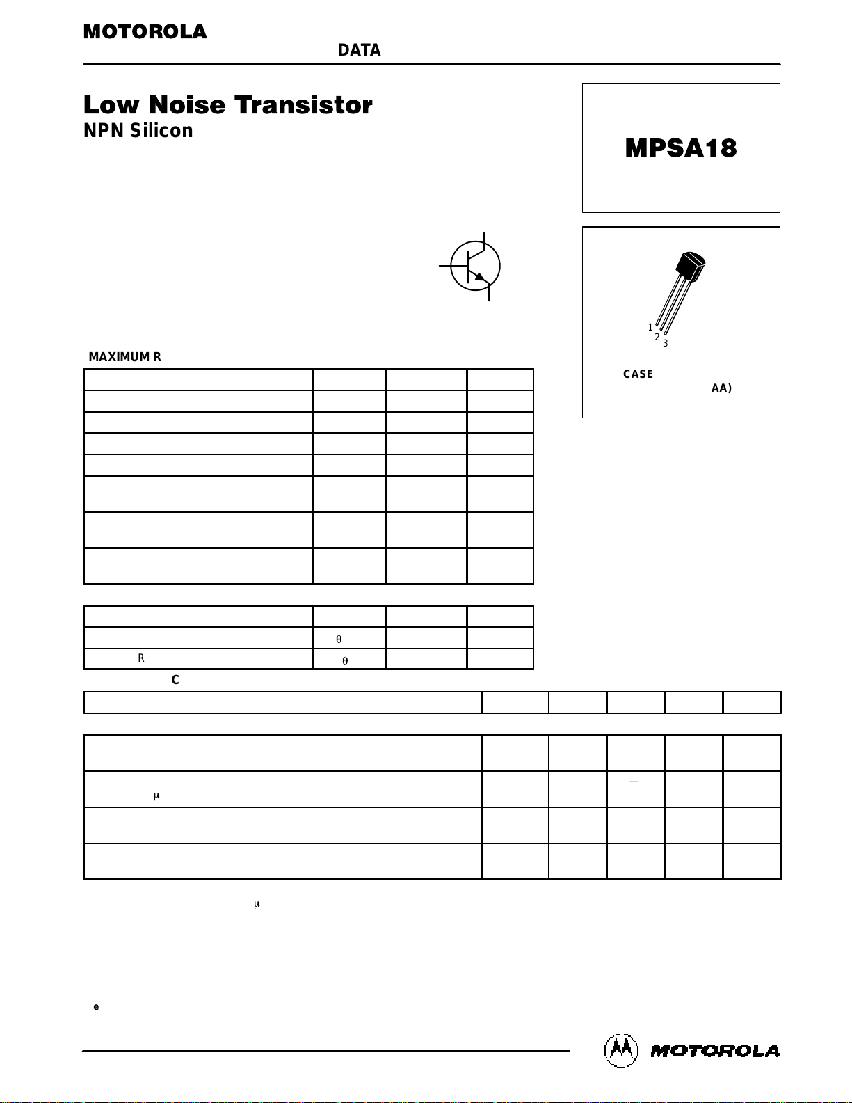
SEMICONDUCTOR TECHNICAL DATA
CASE 29–04, STYLE 1
TO–92 (TO–226AA)
1
2
3
Motorola Preferred Device
Motorola, Inc. 1996
COLLECTOR
3
2
BASE
1
EMITTER
MPSA18
2
Motorola Small–Signal Transistors, FETs and Diodes Device Data
ELECTRICAL CHARACTERISTICS
(TA = 25°C unless otherwise noted) (Continued)
Characteristic
Symbol Min Typ Max Unit
ON CHARACTERISTICS
(2)
DC Current Gain
(IC = 10 µAdc, VCE = 5.0 Vdc)
(IC = 100 µAdc, VCE = 5.0 Vdc)
(IC = 1.0 mAdc, VCE = 5.0 Vdc)
(IC = 10 mAdc, VCE = 5.0 Vdc)
h
FE
400
500
500
500
580
850
1100
1150
—
—
—
1500
—
Collector–Emitter Saturation Voltage
(IC = 10 mAdc, IB = 0.5 mAdc)
(IC = 50 mAdc, IB = 5.0 mAdc)
V
CE(sat)
—
—
—
0.08
0.2
0.3
Vdc
Base–Emitter On Voltage
(IC = 1.0 mAdc, VCE = 5.0 Vdc)
V
BE(on)
— 0.6 0.7 Vdc
SMALL–SIGNAL CHARACTERISTICS
Current–Gain — Bandwidth Product
(IC = 1.0 mAdc, VCE = 5.0 Vdc, f = 100 MHz)
f
T
100 160 — MHz
Collector–Base Capacitance
(VCB = 5.0 Vdc, IE = 0, f = 1.0 MHz)
C
cb
— 1.7 3.0 pF
Emitter–Base Capacitance
(VEB = 0.5 Vdc, IC = 0, f = 1.0 MHz)
C
eb
— 5.6 6.5 pF
Noise Figure
(IC = 100 µAdc, VCE = 5.0 Vdc, RS = 10 kΩ, f = 1.0 kHz)
(IC = 100 µAdc, VCE = 5.0 Vdc, RS = 1.0 kΩ, f = 100 Hz)
NF
—
—
0.5
4.0
1.5
—
dB
Equivalent Short Circuit Noise Voltage
(IC = 100 µAdc, VCE = 5.0 Vdc, RS = 1.0 kΩ, f = 100 Hz)
V
T
— 6.5 —
nVńHz
Ǹ
2. Pulse Test: Pulse Width ≤ 300 ms, Duty Cycle ≤ 2.0%.
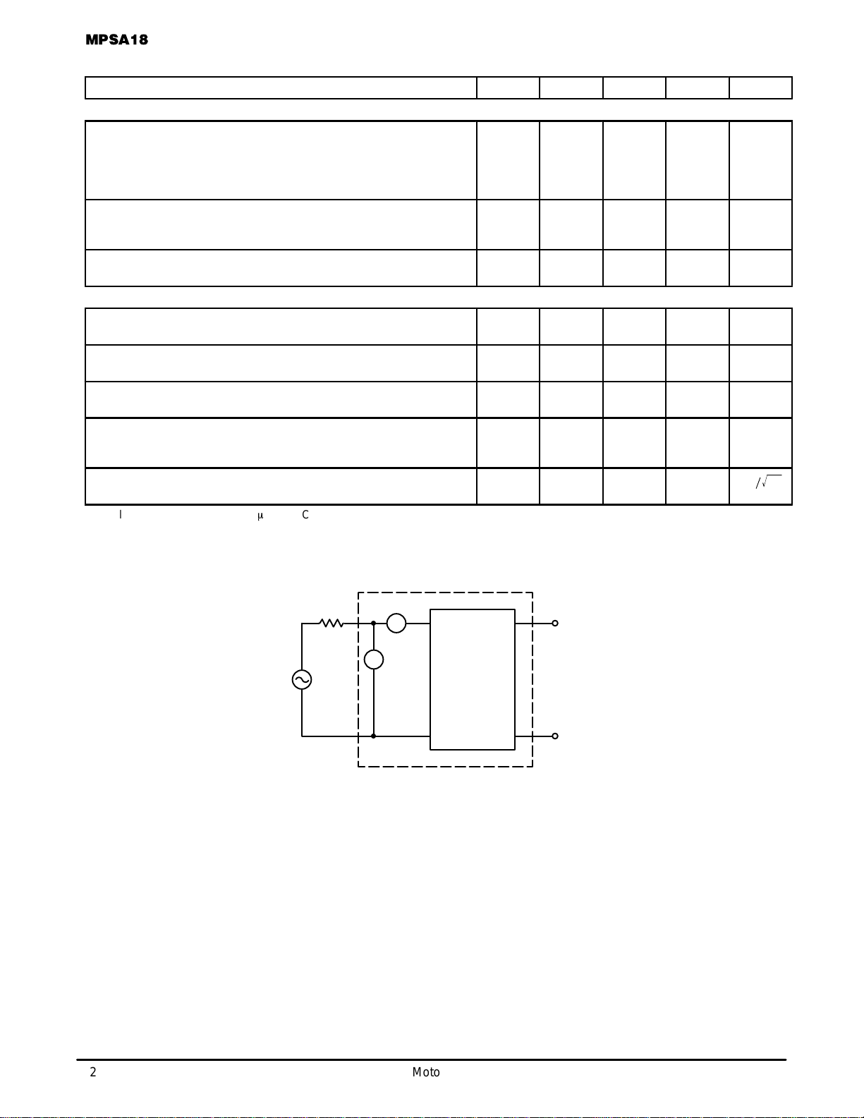
R
S
i
n
e
n
IDEAL
TRANSISTOR
Figure 1. Transistor Noise Model
 Loading...