

Motorola MPC940FA Datasheet
SEMICONDUCTOR TECHNICAL DATA
1
REV 0.2
Motorola, Inc. 1997
6/97
"
!
The MPC940 is a 1:18 low voltage clock distribution chip. The device
features the capability to select either a differential L VPECL or an LVTTL/
LVCMOS compatible input. The 18 outputs are LVCMOS or LVTTL
compatible and feature the drive strength to drive 50Ω series or parallel
terminated transmission lines. With output–to–output skews of 150ps, the
MPC940 is ideal as a clock distribution chip for the most demanding of
synchronous systems. For a similar product with a larger number of
outputs, please consult the MPC941 data sheet.
• LVPECL or LVCMOS/LVTTL Clock Input
• 150ps Maximum Targeted Output–to–Output Skew
• Drives Up to 36 Independent Clock Lines
• Maximum Output Frequency of 250MHz
• 32–Lead TQFP Packaging
• 3.3V V
CC
Supply Voltage
With a low output impedance (≈20Ω), in both the HIGH and LOW logic
states, the output buffers of the MPC940 are ideal for driving series
terminated transmission lines. More specifically, each of the 18 MPC940
outputs can drive two series terminated 50Ω transmission lines. With this
capability, the MPC940 has an effective fanout of 1:36 in applications
where each line drives a single load. With this level of fanout, the
MPC940 provides enough copies of low skew clocks for most high
performance synchronous systems.
The differential LVPECL inputs of the MPC940 allow the device to interface directly with a LVPECL fanout buffer like the
MC100EP111 to build very wide clock fanout trees or to couple to a high frequency clock source. The LVCMOS/LVTTL input
provides a more standard interface for applications requiring only a single clock distribution chip at relatively low frequencies. In
addition, the two clock sources can be used to provide for a test clock interface as well as the primary system clock. A logic HIGH
on the LVCMOS_CLK_Sel pin will select the TTL level clock input.
The MPC940 is fully 3.3V compatible. The 32–lead TQFP package was chosen to optimize performance, board space and
cost of the device. The 32–lead TQFP has a 7x7mm body size with a conservative 0.8mm pin spacing.
This document contains information on a new product. Specifications and information herein are subject to
change without notice.
LOW VOLTAGE
1:18 CLOCK
DISTRIBUTION CHIP
FA SUFFIX
32–LEAD TQFP PACKAGE
CASE 873A–02
MPC940
MOTOROLA TIMING SOLUTIONS
BR1333 — Rev 6
2
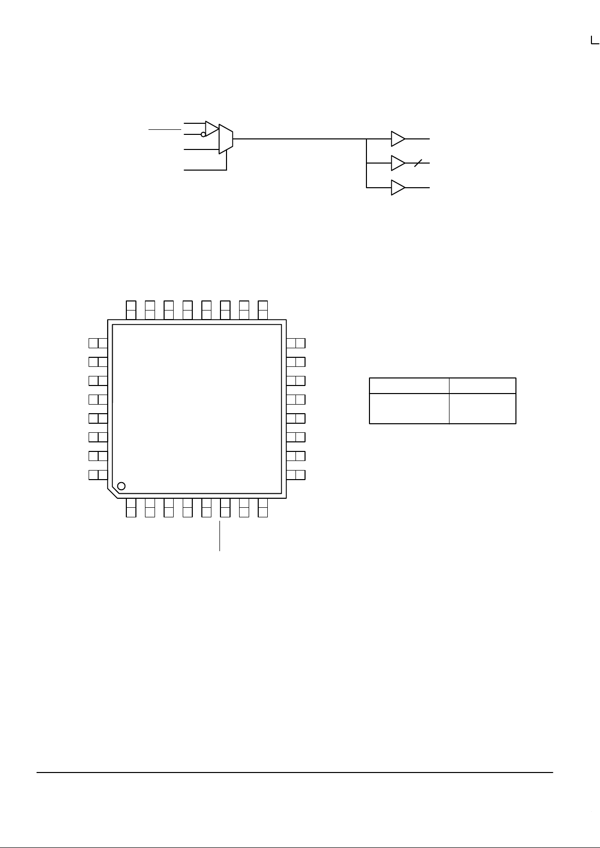
Pinout: 32–Lead TQFP (Top View)
FUNCTION TABLE
LVCMOS_CLK_Sel Input
0
1
PECL_CLK
LVCMOS_CLK
LOGIC DIAGRAM
LVCMOS_CLK
Q0
PECL_CLK
0
1
LVCMOS_CLK_Sel
PECL_CLK
GNDO
Q5
Q4
Q3
VCCO
Q2
Q1
Q0
VCCO
Q12
Q13
Q14
GNDO
Q15
Q16
Q17
Q6
Q7
Q8
VCCOQ9Q10
Q11
GND
GNDO
GNDI
VCCI
LVCMOS_CLK
LVCMOS_CLK_Sel
PECL_CLK
PECL_CLK
VCCO
25
26
27
28
29
30
31
32
15
14
13
12
11
10
9
12345678
24 23 22 21 20 19 18 17
16
MPC940
Q1–Q16
16
Q17
 Loading...