SEMICONDUCTOR TECHNICAL DATA
1
REV 0
Motorola, Inc. 1996
10/96
The MPC9100 is a dual PLL phase locked loop clock generator. The
device synthesizes a 14.318 MHz input reference to provide a buffered
copy of the input reference, a 31.3344MHz clock output and a 45.1584
clock output.
The device features a fully integrated crystal oscillator as the clock
reference source. No external components are required other than the
14.318 MHz crystal. The TCLK input is used only for factory test and
cannot be used as the PLL clock reference. To reduce total die area the
PLL loop filter capacitors are brought outside the chip. The FCAP pins are
used to connect these capacitors to the internal PLL’s. 0.01µf capacitors
are recommended.
The device features three synchronous output enable pins to allow for
shutting down specific clocks. When driven to a logic LOW the OE pins
will freeze the selected clock in its low state. Internal timing has been
established that guarantee transition into and out of the freeze state will
not produce output glitches. These control inputs have internal pull up
resistors so that they will default to the output active state.
The TEST0–2 pins allow for the testing of the internal logic of the
device. Most of the states are reserved for factory test use with one
exception. When the TEST 0 pin is driven low the internal state machines
will be reset and the outputs will be driven into high impedance. The
TEST pins also have internal pull up resistors such that they will default
into the normal operation mode of the chip.
The MPC9100 features separate internal power buses to try to isolate
the output noise from the internal PLL’ s and the other outputs. The VCCA
pins are the power supply pins for the analog PLL’s, the VCCI pin is the
power supply for the internal core logic and the VCCO’s are the power
pins for the output buffers. All of these pins should be tied to a common
power plane on the printed circuit board.
FUNCTION TABLES
TEST2 TEST1 TEST0 Function
0
0
0
0
1
1
1
1
0
0
1
1
0
0
1
1
0
1
0
1
0
1
0
1
Factory Test
Factory Test
Factory Test
Factory Test
Factory Test
Factory Test
Master Reset/Tristate
Normal Operation
OE_XX Function
0
1
Output LOW
Output Active
PIN DESCRIPTION
Pin Description
Q_31
Q_14
Q_45
VCCO_XX
GNDO_XX
VCCI
GNDI
VCCAX
GNDAX
XTAL1
XTAL2
TCLK
FCAPXX
FCAPXXP
31.3344MHz Output
14.318MHz Output
45.1584MHz Output
Output Buffer Power Supply
Output Buffer Ground
Core Logic Power Supply
Core Logic Ground
PLL Power Supply
PLL Ground
Crystal Oscillator Input
Crystal Oscillator Input
LVCMOS Reference Clock Input
PLL Filter Capacitor Input
PLL Filter Capacitor Input
DUAL PLL
CLOCK GENERATOR
FA SUFFIX
TQFP PACKAGE
CASE 873A–02

MPC9100
MOTOROLA TIMING SOLUTIONS
BR1333 — REV 5
2
Q_31
VCCO_31
GNDA1
FCAPB1P
FCAPB1
FCAPA1P
FCAPA1
VCCA1
Q_14
VCCO_14
GNDA2
FCAPB2P
FCAPB2
FCAPA2P
FCAPA2
VCCA2
GND_31
TEST0
TEST1
TEST2
GND_45
Q_45
VCCO_45
GND_14
VCCI
OE_31
OE_45
OE_14
TCLK
XTAL1
XTAL2
GNDI
25
26
27
28
29
30
31
32
15
14
13
12
11
10
9
12345678
24 23 22 21 20 19 18 17
16
MPC9100
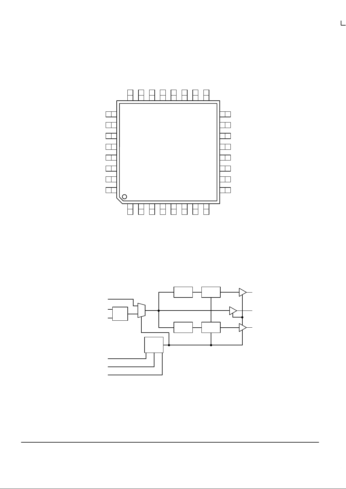
Pinout: 32–Lead TQFP Package (Top View)
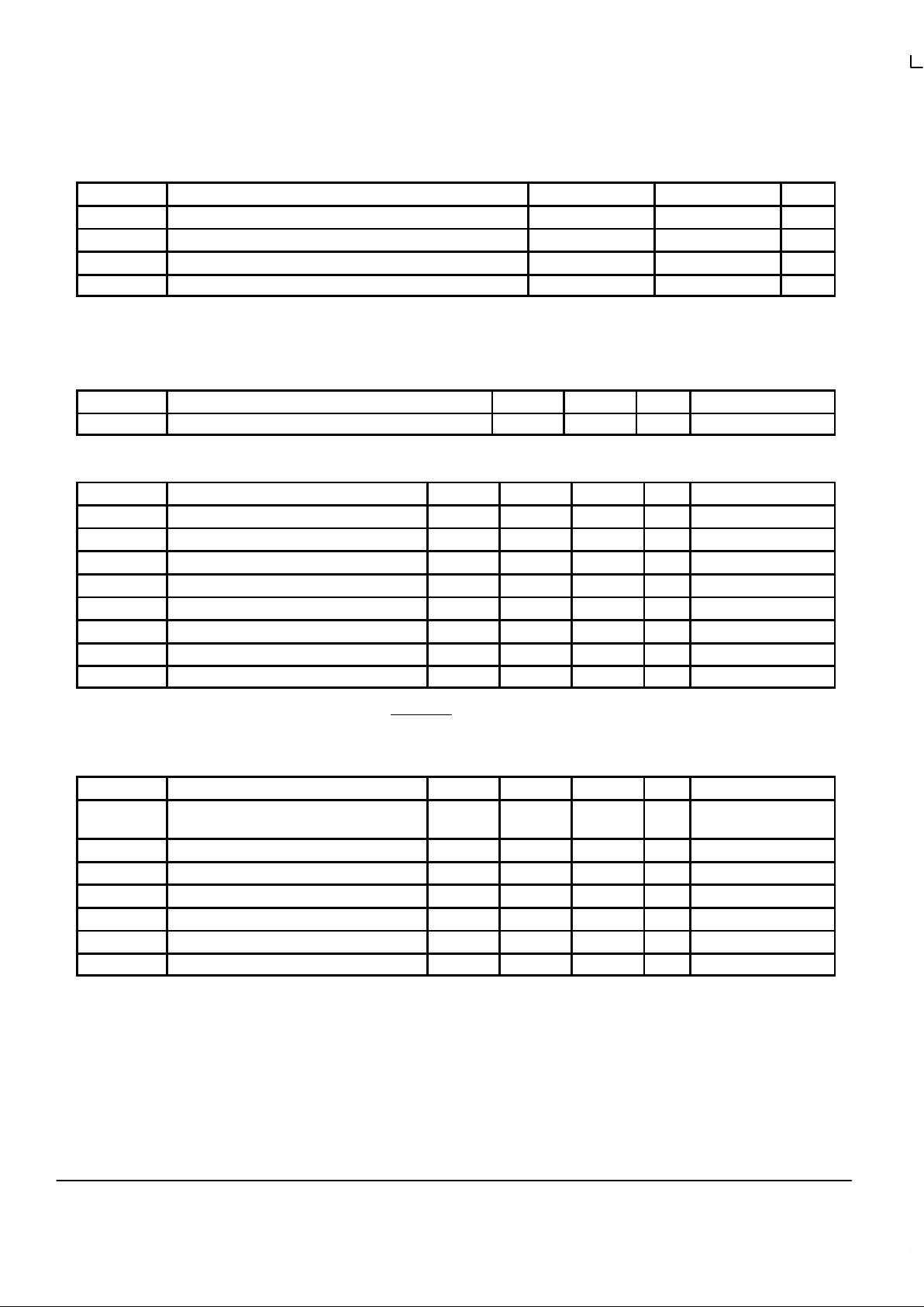
LOGIC DIAGRAM
PLL#1
Q_31
XTAL
OSC
XTAL2
XTAL1
TCLK
TEST0
TEST1
TEST2
Divider
PLL#2 Divider
Q_45
Q_14
TEST
LOGIC

MPC9100
TIMING SOLUTIONS
BR1333 — REV 5
3 MOTOROLA
ABSOLUTE MAXIMUM RATINGS*
Symbol Parameter Min Max Unit
V
CC
Supply Voltage –0.3 4.6 V
V
I
Input Voltage –0.3 VDD + 0.3 V
I
IN
Input Current ±20 mA
T
Stor
Storage Temperature Range –40 125 °C
* Absolute maximum continuous ratings are those values beyond which damage to the device may occur. Exposure to these conditions or
conditions beyond those indicated may adversely affect device reliability. Functional operation under absolute–maximum–rated conditions is
not implied.
PLL INPUT REFERENCE CHARACTERISTICS (TA = 0 to 70°C)
Symbol Characteristic Min Max Unit Condition
f
ref
Reference Input Frequency 10 20 MHz
DC CHARACTERISTICS (TA = 0° to 70°C, VCC = 3.3V ±5%)
Symbol Characteristic Min Typ Max Unit Condition
V
IH
Input HIGH Voltage 2.0 3.6 V
V
IL
Input LOW Voltage 0.8 V
V
OH
Output HIGH Voltage 2.4 V IOH = –20mA
1
V
OL
Output LOW Voltage 0.5 V IOL = 20mA
1
I
IN
Input Current ±120 µA Note 2
I
CC
Maximum Quiescent Supply Current mA
C
IN
4 pF
C
pd
25 pF
1. The MPC9100 outputs can drive series or parallel terminated 50Ω (or 50Ω to VCC/2) transmission lines on the incident edge (see Applications
Info section).
2. Inputs have pull–up resistors which affect input current, PECL_CLK
has a pull–down resistor.
AC CHARACTERISTICS (TA = 0° to 70°C, VCC = 3.3V ±0.3V)
Symbol Characteristic Min Typ Max Unit Condition
tr, t
f
Output Rise/Fall Time 0.15 1.0 ns 0.8 to 2.0V , 50Ω to
VCC/2
t
pw
Output Duty Cycle 45 55 % 50Ω to VCC/2
f
Xtal
Crystal Oscillator Frequency Range 10 20 MHz Note 2
t
PLZ
, t
PHZ
Output Disable Time 2.0 5.0 8.0 ns 50Ω to VCC/2
t
PZL
Output Enable Time 3.0 6.5 10 ns 50Ω to VCC/2
t
jitter
Cycle–to–Cycle Jitter (Peak–to–Peak) ±100 ±250 ps Note 3
t
lock
Maximum PLL Lock Time 10 ms
1. X1, X2, X3, and X4 all to be determined. The specs hold only when the MPC9100 is used in the external feedback mode.
2. See Applications Info section for crystal specifications.
3. All outputs switching.
 Loading...