

Motorola MPC905D, MPC903D, MPC904D Datasheet
SEMICONDUCTOR TECHNICAL DATA
1
REV 3
Motorola, Inc. 1996
10/96
! !
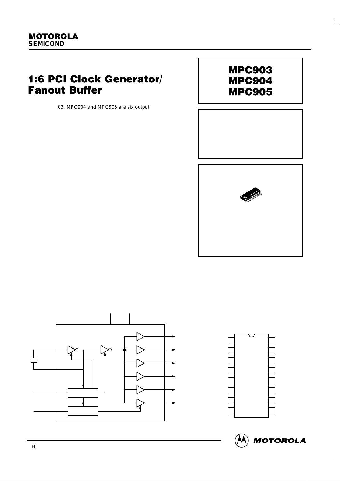
The MPC903, MPC904 and MPC905 are six output clock generation
devices targeted to provide the clocks required in a 3.3V or 5.0V PCI
environment. The device operates from a 3.3V supply and can interface
to either a TTL input or an external crystal. The inputs to the device can be
driven with 5.0V when the VCC is at 3.3V. The outputs of the
MPC903/904/905 meet all of the specifications of the PCI standard. The
three devices are identical except in the function of the Output Enables.
• Six Low Skew Outputs
• Synchronous Output Enables for Power Management
• Low Voltage Operation
• XTAL Oscillator Interface
• 16-Lead SOIC Package
• 5.0V Tolerant Enable Inputs
The MPC903/904/905 device is targeted for PCI bus or processor bus
environments with up to 12 clock loads. Each of the six outputs on the
MPC903/904/905 can drive two series terminated 50Ω transmission
lines. This capability effectively makes the MPC903/904/905 a 1:12
fanout buffer.
The MPC903 offers two synchronous enable inputs to allow users
flexibility in developing power management features for their designs.
Both enable signals are active HIGH inputs. A logic ‘0’ on the Enable1
input will pull all of the outputs into the logic ‘0’ state and shut down the
internal oscillator for a zero power sleep state. A logic ‘0’ on the Enable2
input will disable only the BCLK5 output. The Enable2 input can be used to disable any high power device for system power
savings during periods of inactivity. Both enable inputs are synchronized internal to the chip so that the output disabling will
happen only when the outputs are already LOW. This feature guarantees no runt pulses will be generated during enabling and
disabling. Note that when the MPC903 is re-enabled via the Enable1 pin, the user must allow for the oscillator to regain stability .
Thus, the re-enabling of the chip cannot occur instantaneously. The MPC904 and MPC905 Enable functions are slightly dif ferent
than the 903 and are outlined in the function tables on the following page.
BCLK0
BCLK1
BCLK2
BCLK3
BCLK4
BCLK5
XTAL_IN
XTAL_OUT
Enable1
Enable2
GND (3)VDD (3)
Pinout: 16-Lead Plastic Package (Top View)
161
152
143
134
XTAL_IN
Enable1
BCLK5
V
DD3
XTAL_OUT
Enable2
GND1
BCLK0
125
116
107
98
BCLK4
GND3
BCLK3
V
DD2
V
DD1
BCLK1
GND2
BCLK2
SYNCHRONIZE
SYNCHRONIZE
1:6 PCI
CLOCK GENERATOR/
FANOUT BUFFER
D SUFFIX
PLASTIC SOIC PACKAGE
CASE 751B-05
1
16

MPC903 MPC904 MPC905
MOTOROLA TIMING SOLUTIONS
BR1333 — REV 5
2
FUNCTION TABLE
Outputs 0 to 4 Output 5 OSC (On/Off)
ENABLE1 ENABLE2 MPC903 MPC904 MPC905 MPC903 MPC904 MPC905 MPC903 MPC904 MPC905
0
0
1
1
0
1
0
1
Low
Low
Toggling
Toggling
Low
Low
Toggling
Toggling
Low
Low
Toggling
Toggling
Low
Low
Low
Toggling
Low
Toggling
Low
Toggling
Low
Toggling
Low
Toggling
OFF
OFF
ON
ON
OFF
ON
ON
ON
ON
ON
ON
ON
ABSOLUTE MAXIMUM RATINGS*
Symbol Parameter Min Max Unit
V
DD
Supply Voltage –0.5 4.6 V
V
IN
Input Voltage –0.5 VCC + 0.5 V
T
oper
Operating Temperature Range 0 +70 °C
T
stg
Storage Temperature Range –65 +150 °C
T
sol
Soldering Temperature Range (10 Sec) +260 °C
T
j
Junction Temperature Range +125 °C
P(E1=1) Power Dissipation TBD mW
P(E1=0) Power Dissipation 40 µW
ESD Static Discharge Voltage 2000 V
I
Latch
Latch Up Current 50 mA
* Absolute Maximum Ratings are those values beyond which damage to the device may occur. Functional operation should be restricted to the
Recommended Operating Conditions.
RECOMMENDED OPERATING CONDITIONS
Symbol Parameter Min Max Unit
T
A
Ambient Temperature Range 0 70 °C
V
DD
Positive Supply Voltage (Functional Range) 3.0 3.6 V
tDCin T
high
(at XTAL_IN Input)
T
low
(at XTAL_IN Input)
0.44T
1
0.44T
1
0.56T
1
0.56T
1
T = Period
1. When using External Source for reference, requirement to meet PCI clock duty cycle requirement on the output.
DC CHARACTERISTICS (TA = 0–70°C; VDD = 3.3V ±0.3V)
Symbol Characteristic Min Typ Max Unit Condition
V
IH
High Level Input Voltage 2.0 5.5
2
V
V
IL
Low Level Input Voltage 0.8 V
V
OH
High Level Output Voltage 2.4 V IOH = –36mA
1
V
OL
Low Level Output Voltage 0.4 V IOL = 36mA
1
I
IH
Input High Current 2.5
2
µA
I
IL
Input Low Current 2.5 µA
I
CC
Power Supply Current DC
33MHz
66MHz
20
37
78
45
95
µA
mA
mA
C
IN
Input Capacitance XTAL_IN
Others
9.0
4.5
pF
1. The MPC903/904/905 outputs can drive series terminated or parallel terminated 50Ω (or 50Ω to VCC/2) transmission lines on the incident edge
(see Applications Info).
2. XTAL_IN input will sink up to 10mA when driven to 5.5V . There are no reliability concerns associated with the condition. Note that the Enable1
input must be a logic HIGH. Do not take the Enable1 input to a logic LOW with >VCC volts on the XTAL_IN input.
 Loading...