

MOTOROLA MPC850EC, MPC850ED Technical data

This document contains detailed information on power considerations, AC/DC electrical
characteristics, and AC timing specifications for revision A,B, and C of the MPC850.
This document contains the following topics:
Topic Page
Part I, “Overview” 1
Part II, “Features” 3
Part III, “Electrical and Thermal Characteristics” 7
Part IV, “Thermal Characteristics” 8
Part V, “Power Considerations” 9
Part VI, “Bus Signal Timing” 10
Part VII, “IEEE 1149.1 Electrical Specifications” 37
Part VIII, “CPM Electrical Characteristics” 39
Part IX, “Mechanical Data and Ordering Information” 61
Part X, “Document Revision History” 67
Part I Overview
The MPC850 is a versatile, one-chip integrated microprocessor and peripheral combination
that can be used in a variety of controller applications, excelling particularly in
communications and networking products. The MPC850, which includes support for
Ethernet, is specifically designed for cost-sensitive, remote-access, and telecommunications
applications. It is provides functions similar to the MPC860, with system enhancements such
as universal serial bus (USB) support and a larger (8-Kbyte) dual-port RAM.
In addition to a high-performance embedded MPC8xx core, the MPC850 integrates system
functions, such as a versatile memory controller and a communications processor module
(CPM) that incorporates a specialized, independent RISC communications processor
(referred to as the CP). This separate processor off-loads peripheral tasks from the embedded
MPC8xx core.
The CPM of the MPC850 supports up to seven serial channels, as follows:
• One or two serial communications controllers (SCCs). The SCCs support Ethernet,
ATM (MPC850SAR), HDLC and a number of other protocols, along with a
transparent mode of operation.
Ad vance Information
MPC850EC/D
Rev. 0.2, 04/2002
MPC850 (Rev. A/B/C)
Communications Controller
Hardware Specifications
查询XPC850CZT66B供应商

2
MPC850 (Rev . A/B/C) Har dware Specifications MOT OROLA
• One USB channel
• Two serial management controllers (SMCs)
• One I
2
C port
• One serial peripheral interface (SPI).
Table 1 shows the functionality supported by the members of the MPC850 family.
Additional documentation may be provided for parts listed in Table 1.
Table 1. MPC850 Functionality Matrix
Part
Number of
SCCs
Supported
Ethernet
Support
ATM Support USB Support
Multi-channel
HDLC Support
Number of
PCMCIA Slots
Supported
MPC850 1 Yes - Yes - 1
MPC850DE 2 Yes - Yes - 1
MPC850SAR 2 Yes Yes Yes Yes 1
MOTOROLA
MPC850 (Rev . A/B/C) Har dware Specifications 3
Part II Features
Figure 1 is a block diagram of the MPC850, showing its major components and the relationships among
those components:
Figure 1. MPC850 Microprocessor Block Diagram
The following list summarizes the main features of the MPC850:
• Embedded single-issue, 32-bit MPC8xx core (implementing the PowerPC architecture) with
thirty-two 32-bit general-purpose registers (GPRs)
— Performs branch folding and branch prediction with conditional prefetch, but without
conditional execution
System Interface Unit
Memory Controller
Bus Interface Unit
System Functions
Real-Time Clock
PCMCIA Interface
Bus
Embedded
2-Kbyte
I-Cache
MMU
1-Kbyte
D-Cache
Data
MMU
Load/Store
Instruction
Bus
Parallel I/O
Baud Rate
Generators
Dual-Port
RAM
Interrupt
Controller
Four
Timers
20 Virtual
2 Virtual
32-Bit RISC Communications
Processor (CP) and Program ROM
SCC2
USB
SPI
Timer
Non-Multiplexed Serial Interface
MPC8xx
Core
Instruction
IDMA
Channels
Serial DMA
and
Channels
Unified Bus
Communications
Processor
Module
Peripheral Bus
SCC3
I
2
C
—
UTOPIA
Ports
(850SAR)
SMC1 SMC2
Time Slot Assigner
TDMa

4
MPC850 (Rev . A/B/C) Har dware Specifications MOT OROLA
— 2-Kbyte instruction cache and 1-Kbyte data cache (Harvard architecture)
– Caches are two-way, set-associative
– Physically addressed
– Cache blocks can be updated with a 4-word line burst
– Least-recently used (LRU) replacement algorithm
– Lockable one-line granularity
— Memory management units (MMUs) with 8-entry translation lookaside buffers (TLBs) and
fully-associative instruction and data TLBs
— MMUs support multiple page sizes of 4 Kbytes, 16 Kbytes, 256 Kbytes, 512 Kbytes, and
8 Mbytes; 16 virtual address spaces and eight protection groups
• Advanced on-chip emulation debug mode
• Data bus dynamic bus sizing for 8, 16, and 32-bit buses
— Supports traditional 68000 big-endian, traditional x86 little-endian and modified little-endian
memory systems
— Twenty-six external address lines
• Completely static design (0–80 MHz operation)
• System integration unit (SIU)
— Hardware bus monitor
— Spurious interrupt monitor
— Software watchdog
— Periodic interrupt timer
— Low-power stop mode
— Clock synthesizer
— Decrementer, time base, and real-time clock (RTC) from the PowerPC architecture
— Reset controller
— IEEE 1149.1 test access port (JTAG)
• Memory controller (eight banks)
— Glueless interface to DRAM single in-line memory modules (SIMMs), synchronous DRAM
(SDRAM), static random-access memory (SRAM), electrically programmable read-only
memory (EPROM), flash EPROM, etc.
— Memory controller programmable to support most size and speed memory interfaces
— Boot chip-select available at reset (options for 8, 16, or 32-bit memory)
— Variable block sizes, 32 Kbytes to 256 Mbytes
— Selectable write protection
— On-chip bus arbiter supports one external bus master
— Special features for burst mode support
• General-purpose timers
— Four 16-bit timers or two 32-bit timers
— Gate mode can enable/disable counting

MOTOROLA
MPC850 (Rev . A/B/C) Har dware Specifications 5
— Interrupt can be masked on reference match and event capture
• Interrupts
— Eight external interrupt request (IRQ) lines
— Twelve port pins with interrupt capability
— Fifteen internal interrupt sources
— Programmable priority among SCCs and USB
— Programmable highest-priority request
• Single socket PCMCIA-ATA interface
— Master (socket) interface, release 2.1 compliant
— Single PCMCIA socket
— Supports eight memory or I/O windows
• Communications processor module (CPM)
— 32-bit, Harvard architecture, scalar RISC communications processor (CP)
— Protocol-specific command sets (for example,
GRACEFUL
STOP
TRANSMIT
stops transmission
after the current frame is finished or immediately if no frame is being sent and
CLOSE
RXBD
closes the receive buffer descriptor)
— Supports continuous mode transmission and reception on all serial channels
— Up to 8 Kbytes of dual-port RAM
— Twenty serial DMA (SDMA) channels for the serial controllers, including eight for the four
USB endpoints
— Three parallel I/O registers with open-drain capability
• Four independent baud-rate generators (BRGs)
— Can be connected to any SCC, SMC, or USB
— Allow changes during operation
— Autobaud support option
• Two SCCs (serial communications controllers)
— Ethernet/IEEE 802.3, supporting full 10-Mbps operation
— HDLC/SDLC™
(all channels supported at 2 Mbps)
— HDLC bus (implements an HDLC-based local area network (LAN))
— Asynchronous HDLC to support PPP (point-to-point protocol)
— AppleTalk
®
— Universal asynchronous receiver transmitter (UART)
— Synchronous UART
— Serial infrared (IrDA)
— Totally transparent (bit streams)
— Totally transparent (frame based with optional cyclic redundancy check (CRC))
• QUICC multichannel controller (QMC) microcode features
— Up to 64 independent communication channels on a single SCC
— Arbitrary mapping of 0–31 channels to any of 0–31 TDM time slots

6
MPC850 (Rev . A/B/C) Har dware Specifications MOT OROLA
— Supports either transparent or HDLC protocols for each channel
— Independent TxBDs/Rx and event/interrupt reporting for each channel
• One universal serial bus controller (USB)
— Supports host controller and slave modes at 1.5 Mbps and 12 Mbps
• Two serial management controllers (SMCs)
— UART
— Transparent
— General circuit interface (GCI) controller
— Can be connected to the time-division-multiplexed (TDM) channel
• One serial peripheral interface (SPI)
— Supports master and slave modes
— Supports multimaster operation on the same bus
• One I
2
C
®
(interprocessor-integrated circuit) port
— Supports master and slave modes
— Supports multimaster environment
• Time slot assigner
— Allows SCCs and SMCs to run in multiplexed operation
— Supports T1, CEPT, PCM highway, ISDN basic rate, ISDN primary rate, user-defined
— 1- or 8-bit resolution
— Allows independent transmit and receive routing, frame syncs, clocking
— Allows dynamic changes
— Can be internally connected to four serial channels (two SCCs and two SMCs)
• Low-power support
— Full high: all units fully powered at high clock frequency
— Full low: all units fully powered at low clock frequency
— Doze: core functional units disabled except time base, decrementer, PLL, memory controller,
real-time clock, and CPM in low-power standby
— Sleep: all units disabled except real-time clock and periodic interrupt timer. PLL is active for
fast wake-up
— Deep sleep: all units disabled including PLL, except the real-time clock and periodic interrupt
timer
— Low-power stop: to provide lower power dissipation
— Separate power supply input to operate internal logic at 2.2 V when operating at or below
25 MHz
— Can be dynamically shifted between high frequency (3.3 V internal) and low frequency (2.2 V
internal) operation
• Debug interface
— Eight comparators: four operate on instruction address, two operate on data address, and two
operate on data

MOTOROLA
MPC850 (Rev . A/B/C) Har dware Specifications 7
— The MPC850 can compare using the =, ≠ , <, and > conditions to generate watchpoints
— Each watchpoint can generate a breakpoint internally
• 3.3-V operation with 5-V TTL compatibility on all general purpose I/O pins.
Part III Electrical and Thermal Characteristics
This section provides the AC and DC electrical specifications and thermal characteristics for the MPC850.
Table 2 provides the maximum ratings.
This device contains circuitry protecting against damage due to high-static voltage or electrical fields;
however, it is advised that normal precautions be taken to avoid application of any voltages higher than
maximum-rated voltages to this high-impedance circuit. Reliability of operation is enhanced if unused
inputs are tied to an appropriate logic voltage level (for e xample, either GND or V
CC
). Table 3 provides the
package thermal characteristics for the MPC850.
Table 2. Maximum Ratings
(GND = 0V)
Rating Symbol Value Unit
Supply voltage VDDH -0.3 to 4.0 V
VDDL -0.3 to 4.0 V
KAPWR -0.3 to 4.0 V
VDDSYN -0.3 to 4.0 V
Input voltage
1
1
Functional operating conditions are provided with the DC electrical specifications in Table 5. Absolute maximum
ratings are stress ratings only; functional oper ation at the maxima is not guaranteed. Stress beyond those listed may
affect device reliability or cause permanent damage to the device.
CAUTION: All inputs that tolerate 5 V cannot be more than 2.5 V greater than the supply voltage. This restriction
applies to power-up and normal operation (that is, if the MPC850 is unpowered, v oltage greater than 2.5 V must not
be applied to its inputs).
V
in
GND-0.3 to VDDH + 2.5 V V
Junction temperature
2
2
The MPC850, a high-frequency device in a BGA package, does not provide a guaranteed maximum ambient
temperature. Only maximum junction temperature is guaranteed. It is the responsibility of the user to consider
power dissipation and thermal management. Junction temperature ratings are the same regardless of frequency
rating of the device.
T
j
0 to 95 (standard)
-40 to 95 (extended)
˚C
Storage temperature range T
stg
-55 to +150 ˚C
8
MPC850 (Rev . A/B/C) Har dware Specifications MOT OROLA
Part IV Thermal Characteristics
Table 3 shows the thermal characteristics for the MPC850.
Table 4 provides power dissipation information.
Table 5 provides the DC electrical characteristics for the MPC850.
Table 3. Thermal Characteristics
Characteristic Symbol Value Unit
Thermal resistance for BGA
1
1
For more information on the design of thermal vias on multilayer boards and BGA layout considerations in
general, refer to AN-1231/D,
Plastic Ball Grid Array Application Note
available from y our local Motorola sales
office.
θ
JA
40
2
2
Assumes natural convection and a single layer board (no thermal vias).
°
C/W
θ
JA
31
3
3
Assumes natural convection, a multilayer board with thermal vias
4
, 1 watt MPC850 dissipation, and a board
temperature rise of 20 °
C above ambient.
°
C/W
θ
JA
24
4
4
Assumes natural convection, a multilayer board with thermal vias
4
, 1 watt MPC850 dissipation, and a board
temperature rise of 13 °
C above ambient.
T
J
= T
A
+ (P
D
•
θ
JA
)
P
D
= (V
DD
•
I
DD
) + P
I/O
where:
P
I/O
is the power dissipation on pins
°
C/W
Thermal Resistance for BGA (junction-to-case)
θ
JC
8
° C/W
Table 4. Power Dissipation (P
D
)
Characteristic Frequency (MHz) Typical
1
1
Typical power dissipation is measured at 3.3V
Maximum
2
2
Maximum power dissipation is measured at 3.65 V
Unit
Power Dissipation
All Revisions
(1:1) Mode
33 TBD 515 mW
40 TBD 590 mW
50 TBD 725 mW
Table 5. DC Electrical Specifications
Characteristic Symbol Min Max Unit
Operating voltage at 40 MHz or less VDDH, VDDL,
KAPWR, VDDSYN
3.0 3.6 V
Operating voltage at 40 MHz or higher VDDH, VDDL,
KAPWR, VDDSYN
3.135 3.465 V
Input high voltage (address bus, data bus, EXTAL, EXTCLK,
and all bus control/status signals)
VIH 2.0 3.6 V
Input high voltage (all general purpose I/O and peripheral pins) VIH 2.0 5.5 V

MOTOROLA
MPC850 (Rev . A/B/C) Har dware Specifications 9
Part V Power Considerations
The average chip-junction temperature
,
T
J
,
in ° C can be obtained from the equation:
T
J
= T
A
+ (P
D
•
θ
JA
) (1)
where
T
A
= Ambient temperature
,
°
C
θ
JA
= Package thermal resistance
,
junction to ambient
,
°
C/W
P
D
= P
INT
+ P
I/O
P
INT
= I
DD
x V
DD
, watts—chip internal power
P
I/O
= Power dissipation on input and output pins—user determined
Input low voltage VIL GND 0.8 V
EXTAL, EXTCLK input high voltage VIHC 0.7*(VCC) VCC+0.3 V
Input leakage current, Vin = 5.5 V (Except TMS, TRST
, DSCK
and DSDI pins)
I
in
— 100 µA
Input leakage current, Vin = 3.6V (Except TMS, TRST
, DSCK
and DSDI pins)
I
In
—10µA
Input leakage current, Vin = 0V (Except TMS, TRST
, DSCK and
DSDI pins)
I
In
—10µA
Input capacitance C
in
—20pF
Output high voltage, IOH = -2.0 mA, VDDH = 3.0V
except XTAL, XFC, and open-drain pins
VOH 2.4 — V
Output low voltage
IOL = 2.0 mA CLKOUT
IOL = 3.2 mA
1
IOL = 5.3 mA
2
IOL = 7.0 mA PA[14]/USBOE, PA[12]/TXD2
IOL = 8.9 mA TS
, T A, TEA, BI, BB, HRESET, SRESET
VOL — 0.5 V
1
A[6:31], TSIZ0/REG, TSIZ1, D[0:31], DP[0:3]/IRQ[3:6], RD/WR, BURST, RSV/IRQ2, IP_B[0:1]/IWP[0:1]/VFLS[0:1],
IP_B2/IOIS16_B
/AT2, IP_B3/IWP2/VF2, IP_B4/LWP0/VF0, IP_B5/LWP1/VF1, IP_B6/DSDI/AT0, IP_B7/PTR/AT3,
PA[15]/USBRXD, PA[13]/RXD2, PA[9]/L1TXDA/SMRXD2, PA[8]/L1RXDA/SMTXD2,
PA[7]/CLK1/TIN1/L1RCLKA/BRGO1, PA[6]/CLK2/T
OUT1/TIN3, PA[5]/CLK3/TIN2/L1TCLKA/BRGO2,
PA[4]/CLK4/T
OUT2/TIN4, PB[31]/SPISEL, PB[30]/SPICLK/TXD3, PB[29]/SPIMOSI /RXD3,
PB[28]/SPIMISO/BRGO3, PB[27]/I2CSDA/BRGO1, PB[26]/I2CSCL/BRGO2, PB[25]/SMTXD1/TXD3,
PB[24]/SMRXD1/RXD3, PB[23]/SMSYN1
/SDACK1, PB[22]/SMSYN2/SDACK2, PB[19]/L1ST1,
PB[18]/R
TS2/L1ST2, PB[17]/L1ST3, PB[16]/L1RQa/L1ST4, PC[15]/DREQ0/L1ST5, PC[14]/DREQ1/RTS2/L1ST6,
PC[13]/L1ST7/R
TS3, PC[12]/L1RQa/L1ST8, PC[11]/USBRXP, PC[10]/TGATE1/USBRXN, PC[9]/CTS2,
PC[8]/CD2
/TGATE1, PC[7]/USBTXP, PC[6]/USBTXN, PC[5]/CTS3/L1TSYNCA/SDACK1, PC[4]/CD3/L1RSYNCA,
PD[15], PD[14], PD[13], PD[12], PD[11], PD[10], PD[9], PD[8], PD[7], PD[6], PD[5], PD[4], PD[3]
2
BDIP/GPL_B5, BR, BG, FRZ/IRQ6, CS[0:5], CS6/CE1_B, CS7/CE2_B, WE0/BS_AB0/IORD, WE1/BS_AB1/IOWR,
WE2
/BS_AB2/PCOE, WE3/BS_AB3/PCWE, GPL_A0/GPL_B0, OE/GPL_A1/GPL_B1,
GPL_A
[2:3]/GPL_B[2:3]/CS[2:3], UPWAITA/GPL_A4/AS, UPWAITB/GPL_B4, GPL_A5, ALE_B/DSCK/AT1,
OP2/MODCK1/STS
, OP3/MODCK2/DSDO
Table 5. DC Electrical Specifications (continued)
Characteristic Symbol Min Max Unit

10 MPC850 (Rev . A/B/C) Har dware Specifications MOT OROLA
Layout Practices
For most applications P
I/O
< 0.3
•
P
INT
and can be neglected. If P
I/O
is neglected, an approximate relationship
between P
D
and TJ is:
P
D
= K ÷ (T
J
+ 273°C) (2)
Solving equations (1) and (2) for K gives:
K = P
D
• (T
A
+ 273°C) + θJA • P
D
2
(3)
where K is a constant pertaining to the particular part. K can be determined from equation (3) by measuring
P
D
(at equilibrium) for a known TA. Using this value of K, the values of PD and TJ can be obtained by solving
equations (1) and (2) iteratively for any value of T
A
.
5.1 Layout Practices
Each VCC pin on the MPC850 should be provided with a low-impedance path to the board’s supply. Each
GND pin should likewise be provided with a low-impedance path to ground. The power supply pins drive
distinct groups of logic on chip. The V
CC
power supply should be bypassed to ground using at least four 0.1
µF by-pass capacitors located as close as possible to the four sides of the package. The capacitor leads and
associated printed circuit traces connecting to chip V
CC
and GND should be kept to less than half an inch
per capacitor lead. A four -layer board is recommended, employing two inner layers as V
CC
and GND planes.
All output pins on the MPC850 have fast rise and fall times. Printed circuit (PC) trace interconnection length
should be minimized in order to minimize undershoot and reflections caused by these fast output switching
times. This recommendation particularly applies to the address and data busses. Maximum PC trace lengths
of six inches are recommended. Capacitance calculations should consider all device loads as well as
parasitic capacitances due to the PC traces. Attention to proper PCB layout and bypassing becomes
especially critical in systems with higher capacitive loads because these loads create higher transient
currents in the V
CC
and GND circuits. Pull up all unused inputs or signals that will be inputs during reset.
Special care should be taken to minimize the noise levels on the PLL supply pins.
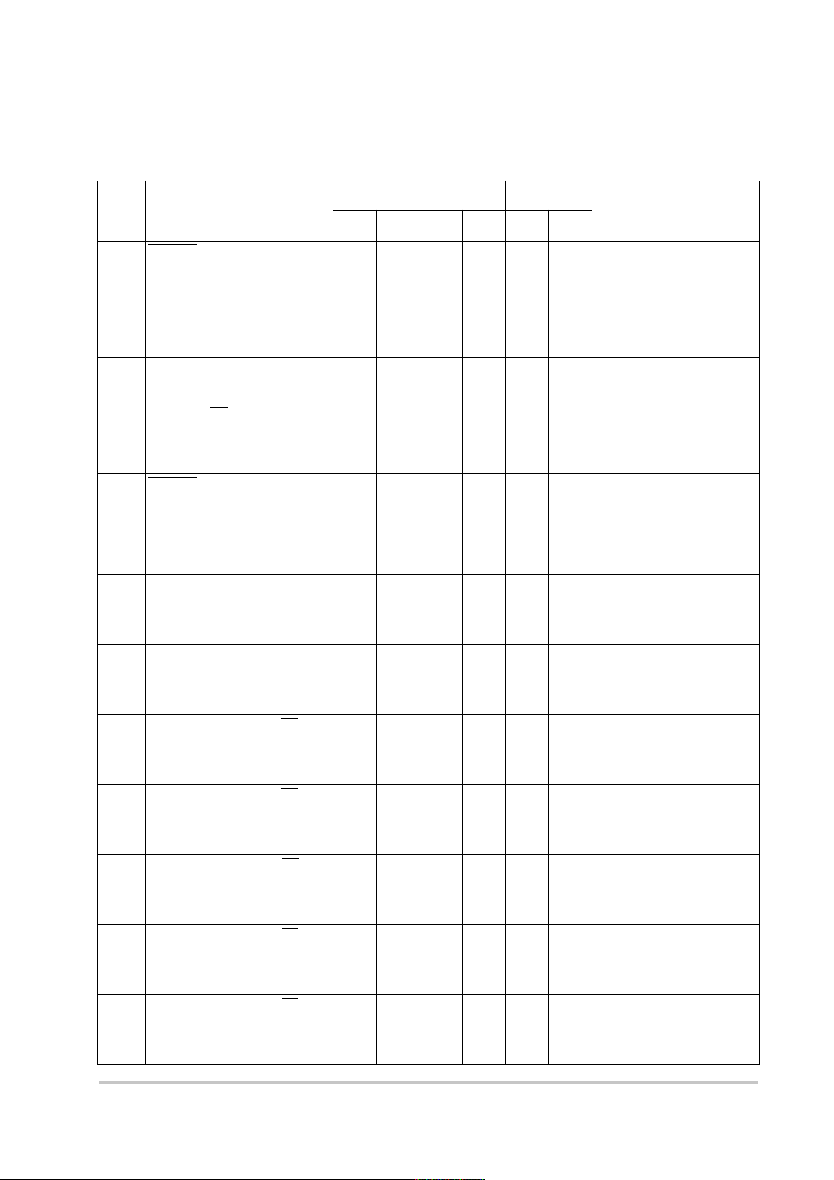
Part VI Bus Signal Timing
Table 6 provides the bus operation timing for the MPC850 at 50 MHz, 66 MHz, and 80 MHz. Timing
information for other bus speeds can be interpolated by equation using the MPC850 Electrical
Specifications Spreadsheet found at http://www.mot.com/netcomm.
The maximum bus speed supported by the MPC850 is 50 MHz. Higher-speed parts must be operated in
half-speed bus mode (for example, an MPC850 used at 66 MHz must be configured for a 33 MHz bus).
The timing for the MPC850 bus shown assumes a 50-pF load. This timing can be derated by 1 ns per 10 pF.
Derating calculations can also be performed using the MPC850 Electrical Specifications Spreadsheet.
MOTOROLA MPC850 (Rev . A/B/C) Har dware Specifications 11
Layout Practices
Table 6. Bus Operation Timing 1
Num Characteristic
50 MHz 66 MHz 80 MHz
FFACT
Cap Load
(default
50 pF)
Unit
Min Max Min Max Min Max
B1 CLKOUT period 20 — 30.30 — 25 — — — ns
B1a EXTCLK to CLKOUT phase
skew (EXTCLK > 15 MHz and
MF <= 2)
-0.90 0.90 -0.90 0.90 -0.90 0.90 — 50.00 ns
B1b EXTCLK to CLKOUT phase
skew (EXTCLK > 10 MHz and
MF < 10)
-2.30 2.30 -2.30 2.30 -2.30 2.30 — 50.00 ns
B1c CLKOUT phase jitter (EXTCLK >
15 MHz and MF <= 2)
2
-0.60 0.60 -0.60 0.60 -0.60 0.60 — 50.00 ns
B1d CLKOUT phase jitter
2
-2.00 2.00 -2.00 2.00 -2.00 2.00 — 50.00 ns
B1e CLKOUT frequency jitter (MF <
10)
2
— 0.50 — 0.50 — 0.50 — 50.00 %
B1f CLKOUT frequency jitter (10 <
MF < 500)
2
— 2.00 — 2.00 — 2.00 — 50.00 %
B1g CLKOUT frequency jitter (MF >
500)
2
— 3.00 — 3.00 — 3.00 — 50.00 %
B1h Frequency jitter on EXTCLK
3
— 0.50 — 0.50 — 0.50 — 50.00 %
B2 CLKOUT pulse width low 8.00 — 12.12 — 10.00 — — 50.00 ns
B3 CLKOUT width high 8.00 — 12.12 — 10.00 — — 50.00 ns
B4 CLKOUT rise time — 4.00 — 4.00 — 4.00 — 50.00 ns
B5 CLKOUT fall time — 4.00 — 4.00 — 4.00 — 50.00 ns
B7 CLKOUT to A[6–31],
RD/WR
, BURST, D[0–31],
DP[0–3] invalid
5.00 — 7.58 — 6.25 — 0.250 50.00 ns
B7a CLKOUT to TSIZ[0–1], REG
,
RSV
, AT[0–3], BDIP, PTR invalid
5.00 — 7.58 — 6.25 — 0.250 50.00 ns
B7b CLKOUT to BR
, BG, FRZ,
VFLS[0–1], VF[0–2] IWP[0–2],
LWP[0–1], STS
invalid
4
5.00 — 7.58 — 6.25 — 0.250 50.00 ns
B8 CLKOUT to A[6–31],
RD/WR
, BURST, D[0–31],
DP[0–3] valid
5.00 11.75 7.58 14.33 6.25 13.00 0.250 50.00 ns
B8a CLKOUT to TSIZ[0–1], REG
,
RSV
, AT[0–3] BDIP, PTR valid
5.00 11.75 7.58 14.33 6.25 13.00 0.250 50.00 ns
B8b CLKOUT to BR
, BG, VFLS[0–1],
VF[0–2], IWP[0–2], FRZ,
LWP[0–1], STS
valid
4
5.00 11.74 7.58 14.33 6.25 13.00 0.250 50.00 ns
B9 CLKOUT to A[6–31] RD/WR
,
B
URST, D[0–31], DP[0–3],
TSIZ[0–1], REG
, RSV, AT[0–3],
PTR
high-Z
5.00 11.75 7.58 14.33 6.25 13.00 0.250 50.00 ns
12 MPC850 (Rev . A/B/C) Har dware Specifications MOT OROLA
Layout Practices
B11 CLKOUT to TS, BB assertion 5.00 11.00 7.58 13.58 6.25 12.25 0.250 50.00 ns
B11a CLKOUT to T
A, BI assertion,
(When driven by the memory
controller or PCMCIA interface)
2.50 9.25 2.50 9.25 2.50 9.25 — 50.00 ns
B12 CLKOUT to TS
, BB negation 5.00 11.75 7.58 14.33 6.25 13.00 0.250 50.00 ns
B12a CLKOUT to T
A, BI negation
(when driven by the memory
controller or PCMCIA interface)
2.50 11.00 2.50 11.00 2.50 11.00 — 50.00 ns
B13 CLKOUT to TS
, BB high-Z 5.00 19.00 7.58 21.58 6.25 20.25 0.250 50.00 ns
B13a CLK OUT to T
A, BI high-Z, (when
driven by the memory controller
or PCMCIA interface)
2.50 15.00 2.50 15.00 2.50 15.00 — 50.00 ns
B14 CLKOUT to TEA
assertion 2.50 10.00 2.50 10.00 2.50 10.00 — 50.00 ns
B15 CLKOUT to TEA
high-Z 2.50 15.00 2.50 15.00 2.50 15.00 — 50.00 ns
B16 T
A, BI valid to CLKOUT(setup
time)
5
9.75 — 9.75 — 9.75 — — 50.00 ns
B16a TEA
, KR, RETRY, valid to
CLKOUT (setup time
) 5
10.00 — 10.00 — 10.00 — — 50.00 ns
B16b BB
, BG, BR valid to CLKOUT
(setup time)
6
8.50 — 8.50 — 8.50 — — 50.00 ns
B17 CLKOUT to T
A, TEA, BI, BB, BG,
BR
valid (Hold time).
5
1.00 — 1.00 — 1.00 — — 50.00 ns
B17a CLKOUT to KR
, RETRY, except
TEA
valid (hold time)
2.00 — 2.00 — 2.00 — — 50.00 ns
B18 D[0–31], DP[0–3] valid to
CLKOUT rising edge (setup
time)
7
6.00 — 6.00 — 6.00 — — 50.00 ns
B19 CLKOUT rising edge to D[0–31],
DP[0–3] valid (hold time)
7
1.00 — 1.00 — 1.00 — — 50.00 ns
B20 D[0–31], DP[0–3] valid to
CLKOUT falling edge (setup
time)
8
4.00 — 4.00 — 4.00 — — 50.00 ns
B21 CLKOUT f alling edge to D[0–31],
DP[0–3] valid (hold time)
8
2.00 — 2.00 — 2.00 — — — —
B22 CLKOUT rising edge to CS
asserted GPCM ACS = 00
5.00 11.75 7.58 14.33 6.25 13.00 0.250 50.00 ns
B22a CLKOUT falling edge to CS
asserted GPCM ACS = 10, TRLX
= 0,1
— 8.00 — 8.00 — 8.00 — 50.00 ns
B22b CLKOUT falling edge to CS
asserted GPCM ACS = 11, TRLX
= 0, EBDF = 0
5.00 11.75 7.58 14.33 6.25 13.00 0.250 50.00 ns
Table 6. Bus Operation Timing 1 (continued)
Num Characteristic
50 MHz 66 MHz 80 MHz
FFACT
Cap Load
(default
50 pF)
Unit
Min Max Min Max Min Max

MOTOROLA MPC850 (Rev . A/B/C) Har dware Specifications 13
Layout Practices
B22c CLKOUT falling edge to CS
asserted GPCM ACS = 11, TRLX
= 0, EBDF = 1
7.00 14.00 11.00 18.00 9.00 16.00 0.375 50.00 ns
B23 CLKOUT rising edge to CS
negated GPCM read access,
GPCM write access ACS = 00,
TRLX = 0 & CSNT = 0
2.00 8.00 2.00 8.00 2.00 8.00 — 50.00 ns
B24 A[6–31] to CS
asserted GPCM
ACS = 10, TRLX = 0.
3.00 — 6.00 — 4.00 — 0.250 50.00 ns
B24a A[6–31] to CS
asserted GPCM
ACS = 11, TRLX = 0
8.00 — 13.00 — 11.00 — 0.500 50.00 ns
B25 CLKOUT rising edge to OE
,
WE[0–3]
asserted
— 9.00 — 9.00 — 9.00 — 50.00 ns
B26 CLKOUT rising edge to OE
negated
2.00 9.00 2.00 9.00 2.00 9.00 — 50.00 ns
B27 A[6–31] to CS
asserted GPCM
ACS = 10, TRLX = 1
23.00 — 36.00 — 29.00 — 1.250 50.00 ns
B27a A[6–31] to CS
asserted GPCM
ACS = 11, TRLX = 1
28.00 — 43.00 — 36.00 — 1.500 50.00 ns
B28 CLKOUT rising edge to WE[0–3]
negated GPCM write access
CSNT = 0
— 9.00 — 9.00 — 9.00 — 50.00 ns
B28a CLKOUT falling edge to WE[0–3]
negated GPCM write access
TRLX = 0,1 CSNT = 1, EBDF = 0
5.00 12.00 8.00 14.00 6.00 13.00 0.250 50.00 ns
B28b CLKOUT falling edge to CS
negated GPCM write access
TRLX = 0,1 CSNT = 1, ACS = 10
or ACS = 11, EBDF = 0
— 12.00 — 14.00 — 13.00 0.250 50.00 ns
B28c CLKOUT f alling edge to WE[0–3]
negated GPCM write access
TRLX = 0,1 CSNT = 1 write
access TRLX = 0, CSNT = 1,
EBDF = 1
7.00 14.00 11.00 18.00 9.00 16.00 0.375 50.00 ns
B28d CLKOUT falling edge to CS
negated GPCM write access
TRLX = 0,1 CSNT = 1, ACS = 10
or ACS = 11, EBDF = 1
— 14.00 — 18.00 — 16.00 0.375 50.00 ns
B29 WE[0–3]
negated to D[0–31],
DP[0–3] high-Z GPCM write
access, CSNT = 0
3.00 — 6.00 — 4.00 — 0.250 50.00 ns
B29a WE[0–3]
negated to D[0–31],
DP[0–3] high-Z GPCM write
access, TRLX = 0 CSNT = 1,
EBDF = 0
8.00 — 13.00 — 11.00 — 0.500 50.00 ns
Table 6. Bus Operation Timing 1 (continued)
Num Characteristic
50 MHz 66 MHz 80 MHz
FFACT
Cap Load
(default
50 pF)
Unit
Min Max Min Max Min Max

14 MPC850 (Rev . A/B/C) Har dware Specifications MOT OROLA
Layout Practices
B29b CS negated to D[0–31], DP[0–3],
high-Z GPCM write access, ACS
= 00, TRLX = 0 & CSNT = 0
3.00 — 6.00 — 4.00 — 0.250 50.00 ns
B29c CS
negated to D[0–31], DP[0–3]
high-Z GPCM write access,
TRLX = 0, CSNT = 1, ACS = 10
or ACS = 11, EBDF = 0
8.00 — 13.00 — 11.00 — 0.500 50.00 ns
B29d WE[0–3]
negated to D[0–31],
DP[0–3] high-Z GPCM write
access, TRLX = 1, CSNT = 1,
EBDF = 0
28.00 — 43.00 — 36.00 — 1.500 50.00 ns
B29e CS
negated to D[0–31], DP[0–3]
high-Z GPCM write access,
TRLX = 1, CSNT = 1, ACS = 10
or ACS = 11, EBDF = 0
28.00 — 43.00 — 36.00 — 1.500 50.00 ns
B29f WE[0–3]
negated to D[0–31],
DP[0–3] high-Z GPCM write
access TRLX = 0, CSNT = 1,
EBDF = 1
5.00 — 9.00 — 7.00 — 0.375 50.00 ns
B29g CS
negated to D[0–31], DP[0–3]
high-Z GPCM write access TRLX
= 0, CSNT = 1, ACS = 10 or ACS
= 11, EBDF = 1
5.00 — 9.00 — 7.00 — 0.375 50.00 ns
B29h WE[0–3]
negated to D[0–31],
DP[0–3] high-Z GPCM write
access TRLX = 0, CSNT = 1,
EBDF = 1
25.00 — 39.00 — 31.00 — 1.375 50.00 ns
B29i CS
negated to D[0–31], DP[0–3]
high-Z GPCM write access,
TRLX = 1, CSNT = 1, ACS = 10
or ACS = 11, EBDF = 1
25.00 — 39.00 — 31.00 — 1.375 50.00 ns
B30 CS
, WE[0–3] negated to A[6–31]
invalid
GPCM write access
9
3.00 — 6.00 — 4.00 — 0.250 50.00 ns
B30a WE[0–3]
negated to A[6–31]
invalid
GPCM write access, TRLX = 0,
CSNT = 1, CS
negated to
A[6–31] invalid GPCM write
access TRLX = 0, CSNT =1,
ACS = 10 or ACS = 11, EBDF = 0
8.00 — 13.00 — 11.00 — 0.500 50.00 ns
Table 6. Bus Operation Timing 1 (continued)
Num Characteristic
50 MHz 66 MHz 80 MHz
FFACT
Cap Load
(default
50 pF)
Unit
Min Max Min Max Min Max
MOTOROLA MPC850 (Rev . A/B/C) Har dware Specifications 15
Layout Practices
B30b WE[0–3] negated to A[6–31]
invalid
GPCM write access, TRLX = 1,
CSNT = 1. CS
negated to
A[6–31] Invalid GPCM write
access TRLX = 1, CSNT = 1,
ACS = 10 or ACS = 11, EBDF = 0
28.00 — 43.00 — 36.00 — 1.500 50.00 ns
B30c WE[0–3]
negated to A[6–31]
invalid
GPCM write access, TRLX = 0,
CSNT = 1. CS
negated to
A[6–31] invalid GPCM write
access, TRLX = 0, CSNT = 1,
ACS = 10 or ACS = 11, EBDF = 1
5.00 — 8.00 — 6.00 — 0.375 50.00 ns
B30d WE[0–3]
negated to A[6–31]
invalid GPCM write access TRLX
= 1, CSNT =1, CS
negated to
A[6–31] invalid GPCM write
access TRLX = 1, CSNT = 1,
ACS = 10 or ACS = 11, EBDF = 1
25.00 — 39.00 — 31.00 — 1.375 50.00 ns
B31 CLKOUT f alling edge to CS
valid
- as requested by control bit
CST4 in the corresponding word
in the UPM
1.50 6.00 1.50 6.00 1.50 6.00 — 50.00 ns
B31a CLKOUT falling edge to CS
valid
- as requested by control bit
CST1 in the corresponding word
in the UPM
5.00 12.00 8.00 14.00 6.00 13.00 0.250 50.00 ns
B31b CLKOUT rising edge to CS
valid
- as requested by control bit
CST2 in the corresponding word
in the UPM
1.50 8.00 1.50 8.00 1.50 8.00 — 50.00 ns
B31c CLKOUT rising edge to CS
valid
- as requested by control bit
CST3 in the corresponding word
in the UPM
5.00 12.00 8.00 14.00 6.00 13.00 0.250 50.00 ns
B31d CLKOUT falling edge to CS
valid
- as requested by control bit
CST1 in the corresponding word
in the UPM EBDF = 1
9.00 14.00 13.00 18.00 11.00 16.00 0.375 50.00 ns
B32 CLKOUT f alling edge to BS
valid
- as requested by control bit
BST4 in the corresponding word
in the UPM
1.50 6.00 1.50 6.00 1.50 6.00 — 50.00 ns
B32a CLKOUT falling edge to BS
valid
- as requested by control bit
BST1 in the corresponding word
in the UPM, EBDF = 0
5.00 12.00 8.00 14.00 6.00 13.00 0.250 50.00 ns
Table 6. Bus Operation Timing 1 (continued)
Num Characteristic
50 MHz 66 MHz 80 MHz
FFACT
Cap Load
(default
50 pF)
Unit
Min Max Min Max Min Max

16 MPC850 (Rev . A/B/C) Har dware Specifications MOT OROLA
Layout Practices
B32b CLKOUT rising edge to BS valid
- as requested by control bit
BST2 in the corresponding word
in the UPM
1.50 8.00 1.50 8.00 1.50 8.00 — 50.00 ns
B32c CLKOUT rising edge to BS
valid
- as requested by control bit
BST3 in the corresponding word
in the UPM
5.00 12.00 8.00 14.00 6.00 13.00 0.250 50.00 ns
B32d CLKOUT falling edge to BS
valid
- as requested by control bit
BST1 in the corresponding word
in the UPM, EBDF = 1
9.00 14.00 13.00 18.00 11.00 16.00 0.375 50.00 ns
B33 CLKOUT falling edge to GPL
valid - as requested by control bit
GxT4 in the corresponding word
in the UPM
1.50 6.00 1.50 6.00 1.50 6.00 — 50.00 ns
B33a CLKOUT rising edge to GPL
valid - as requested by control bit
GxT3 in the corresponding word
in the UPM
5.00 12.00 8.00 14.00 6.00 13.00 0.250 50.00 ns
B34 A[6–31] and D[0–31] to CS
valid
- as requested by control bit
CST4 in the corresponding word
in the UPM
3.00 — 6.00 — 4.00 — 0.250 50.00 ns
B34a A[6–31] and D[0–31] to CS
valid
- as requested by control bit
CST1 in the corresponding word
in the UPM
8.00 — 13.00 — 11.00 — 0.500 50.00 ns
B34b A[6–31] and D[0–31] to CS
valid
- as requested by CST2 in the
corresponding word in UPM
13.00 — 21.00 — 17.00 — 0.750 50.00 ns
B35 A[6–31] to CS
valid - as
requested by control bit BST4 in
the corresponding word in UPM
3.00 — 6.00 — 4.00 — 0.250 50.00 ns
B35a A[6–31] and D[0–31] to BS
valid
- as requested by BST1 in the
corresponding word in the UPM
8.00 — 13.00 — 11.00 — 0.500 50.00 ns
B35b A[6–31] and D[0–31] to BS
valid
- as requested by control bit
BST2 in the corresponding word
in the UPM
13.00 — 21.00 — 17.00 — 0.750 50.00 ns
B36 A[6–31] and D[0–31] to GPL
valid - as requested by control bit
GxT4 in the corresponding word
in the UPM
3.00 — 6.00 — 4.00 — 0.250 50.00 ns
Table 6. Bus Operation Timing 1 (continued)
Num Characteristic
50 MHz 66 MHz 80 MHz
FFACT
Cap Load
(default
50 pF)
Unit
Min Max Min Max Min Max

MOTOROLA MPC850 (Rev . A/B/C) Har dware Specifications 17
Layout Practices
B37 UPWAIT v alid to CLK OUT falling
edge
10
6.00 — 6.00 — 6.00 — — 50.00 ns
B38 CLKOUT f alling edge to UPWAIT
valid
10
1.00 — 1.00 — 1.00 — — 50.00 ns
B39 AS
valid to CLK OUT rising edge
11
7.00 — 7.00 — 7.00 — — 50.00 ns
B40 A[6–31], TSIZ[0–1], RD/WR
,
B
URST, valid to CLKOUT rising
edge.
7.00 — 7.00 — 7.00 — — 50.00 ns
B41 TS
valid to CLKOUT rising edge
(setup time)
7.00 — 7.00 — 7.00 — — 50.00 ns
B42 CLKOUT rising edge to TS
valid
(hold time)
2.00 — 2.00 — 2.00 — — 50.00 ns
B43 AS
negation to memory
controller signals negation
— TBD — TBD TBD — — 50.00 ns
1
The minima provided assume a 0 pF load, whereas maxima assume a 50pF load. F or frequencies not marked on the
part, new bus timing must be calculated for all frequency-dependent AC parameters. Frequency-dependent AC
parameters are those with an entry in the FFactor column. A C parameters without an FFactor entry do not need to be
calculated and can be taken directly from the frequency column corresponding to the frequency marked on the part.
The following equations should be used in these calculations.
For a frequency F, the following equations should be applied to each one of the above parameters:
For minima:
For maxima:
where:
D is the parameter value to the frequency required in ns
F is the operation frequency in MHz
D
50
is the parameter value defined for 50 MHz
CAP LOAD is the capacitance load on the signal in question.
FFACTOR is the one defined for each of the parameters in the table.
2
Phase and frequency jitter performance results are valid only if the input jitter is less than the prescribed value.
3
If the rate of change of the frequency of EXTAL is slow (i.e. it does not jump between the minimum and maximum
values in one cycle) or the frequency of the jitter is fast (i.e., it does not stay at an extreme value f or a long time) then
the maximum allowed jitter on EXTAL can be up to 2%.
4
The timing for BR output is relev ant when the MPC850 is selected to work with e xternal bus arbiter . The timing for BG
output is relevant when the MPC850 is selected to work with internal bus arbiter.
5
The setup times required for TA, TEA, and BI are relevant only when the y are supplied b y an e xternal device (and not
when the memory controller or the PCMCIA interface drives them).
6
The timing required for BR input is relevant when the MPC850 is selected to work with the internal bus arbiter. The
timing for BG
input is relevant when the MPC850 is selected to work with the external bus arbiter.
7
The D[0–31] and DP[0–3] input timings B20 and B21 refer to the rising edge of the CLKOUT in which the TA input
signal is asserted.
Table 6. Bus Operation Timing 1 (continued)
Num Characteristic
50 MHz 66 MHz 80 MHz
FFACT
Cap Load
(default
50 pF)
Unit
Min Max Min Max Min Max
D =
FFACTOR x 1000
F
(D
50
- 20 x FFACTOR)
+
D =
FFACTOR x 1000F(D
50
-20 x FFACTOR)
++
1ns(CAP LOAD - 50) / 10

18 MPC850 (Rev . A/B/C) Har dware Specifications MOT OROLA
Layout Practices
Figure 2 is the control timing diagram.
Figure 2. Control Timing
8
The D[0:31] and DP[0:3] input timings B20 and B21 refer to the falling edge of CLKOUT. This timing is valid only for
read accesses controlled by chip-selects controlled by the UPM in the memory controller, for data beats where DLT3
= 1 in the UPM RAM words. (This is only the case where data is latched on the falling edge of CLKOUT.
9
The timing B30 refers to CS when ACS = '00' and to WE[0:3] when CSNT = '0'.
10
The signal UPWAIT is considered asynchronous to CLKOUT and synchronized internally. The timings specified in
B37 and B38 are specified to enable the freeze of the UPM output signals.
11
The AS signal is considered asynchronous to CLKOUT.
CLKOUT
Outputs
A
B
2.0 V
0.8 V
0.8 V
2.0 V
2.0 V
0.8 V
2.0 V
0.8 V
Outputs
2.0 V
0.8 V
2.0 V
0.8 V
B
A
Inputs
2.0 V
0.8 V
2.0 V
0.8 V
D
C
Inputs
2.0 V
0.8 V
2.0 V
0.8 V
C
D
A Maximum output delay specification
B Minimum output hold time
C Minimum input setup time specification
D Minimum input hold time specification

MOTOROLA MPC850 (Rev . A/B/C) Har dware Specifications 19
Layout Practices
Figure 3 provides the timing for the external clock.
Figure 3. External Clock Timing
Figure 4 provides the timing for the synchronous output signals.
Figure 4. Synchronous Output Signals Timing
CLKOUT
B1
B5
B3
B4
B1
B2
CLKOUT
Output
Signals
Output
Signals
Output
Signals
B8
B7 B9
B8a
B9B7a
B8b
B7b

20 MPC850 (Rev . A/B/C) Har dware Specifications MOT OROLA
Layout Practices
Figure 5 provides the timing for the synchronous active pull-up and open-drain output signals.
Figure 5. Synchronous Active Pullup and Open-Drain Outputs Signals Timing
Figure 6 provides the timing for the synchronous input signals.
Figure 6. Synchronous Input Signals Timing
CLKOUT
TS
, BB
TA, BI
TEA
B13
B12B11
B11a
B12a
B13a
B15
B14
CLKOUT
T
A, BI
TEA, KR,
RETR
Y
BB, BG, BR
B16
B17
B16a
B17a
B16b
B17
MOTOROLA MPC850 (Rev . A/B/C) Har dware Specifications 21
Layout Practices
Figure 7 provides normal case timing for input data.
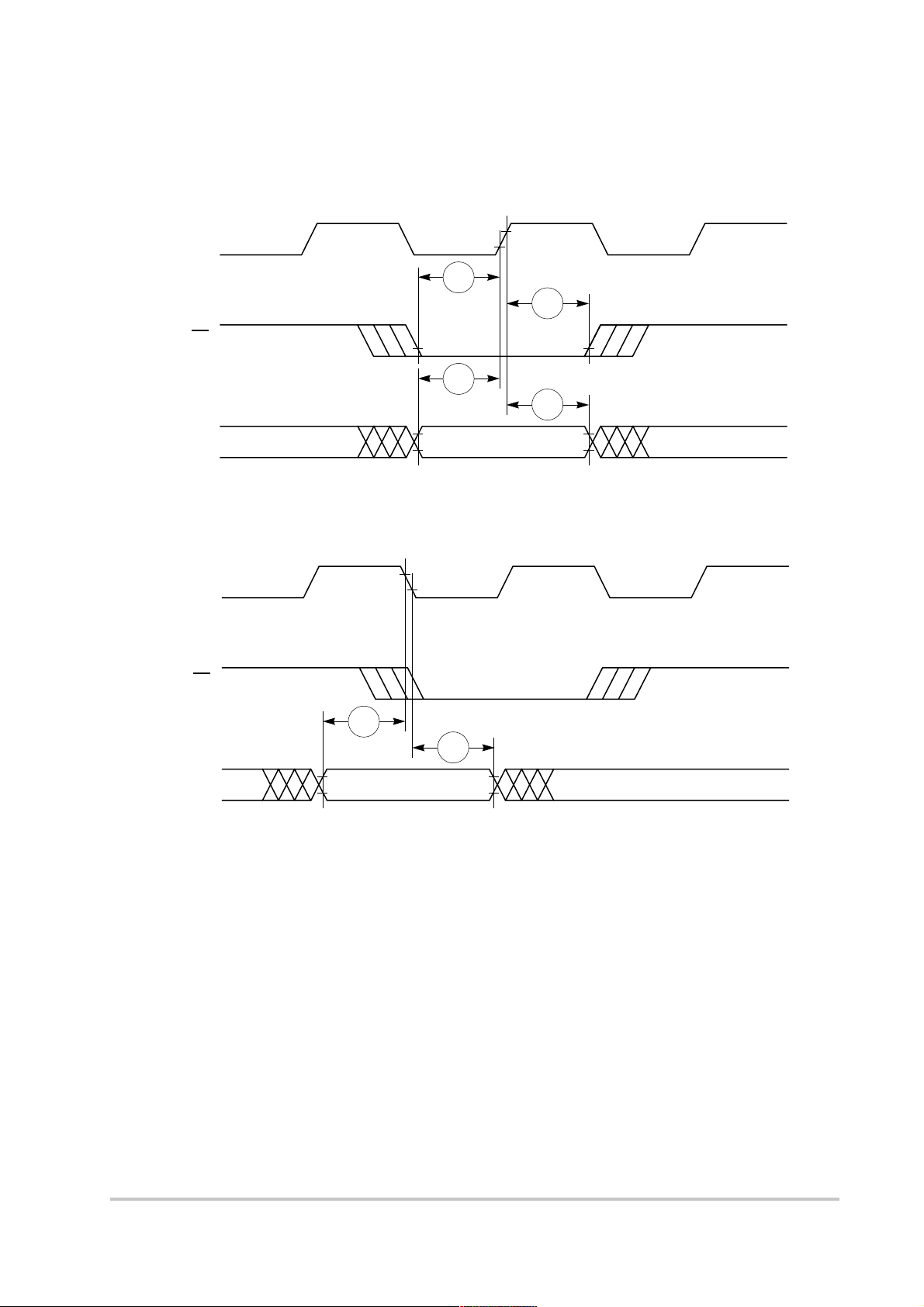
Figure 7. Input Data Timing in Normal Case
Figure 8 provides the timing for the input data controlled by the UPM in the memory controller.
Figure 8. Input Data Timing when Controlled by UPM in the Memory Controller
CLKOUT
T
A
D[0:31],
DP[0:3]
B16
B17
B19
B18
CLKOUT
T
A
D[0:31],
DP[0:3]
B20
B21
 Loading...