

Motorola MOC223 Datasheet
1
Motorola Optoelectronics Device Data
Darlington Output
These devices consist of a gallium arsenide infrared emitting diode optically
coupled to a monolithic silicon photodarlington detector, in a surface mountable,
small outline, plastic package. They are ideally s uited for high density
applications, and eliminate the need for through–the–board mounting.
• Convenient Plastic SOIC–8 Surface Mountable Package Style
• High Current Transfer Ratio (CTR) at Low LED Input Current, for Easier Logic
Interfacing
• Standard SOIC–8 Footprint, with 0.050″ Lead Spacing
• Shipped in Tape and Reel, which Conforms to EIA Standard RS481A
• Compatible with Dual Wave, Vapor Phase and IR Reflow Soldering
• High Input–Output Isolation of 3000 Vac (rms) Guaranteed
• UL Recognized
File #E54915
Ordering Information:
• To obtain MOC223 in Tape and Reel, add R2 suffix to device numbers:
R2 = 2500 units on 13″ reel
• To obtain MOC223 in quantities of 50 (shipped in sleeves) — No Suffix
Marking Information:
• MOC223 = 223
Applications:
• Low power Logic Circuits
• Interfacing and coupling systems of different potentials and impedances
• Telecommunications equipment
• Portable electronics
MAXIMUM RATINGS (T
A
= 25°C unless otherwise noted)
Rating Symbol Value Unit
INPUT LED
Forward Current — Continuous I
F
60 mA
Forward Current — Peak (PW = 100 µs, 120 pps) IF(pk) 1.0 A
Reverse Voltage V
R
6.0 V
LED Power Dissipation @ TA = 25°C
Derate above 25°C
P
D
90
0.8
mW
mW/°C
OUTPUT DARLINGTON
Collector–Emitter Voltage V
CEO
30 V
Collector–Base Voltage V
CBO
70 V
Emitter–Collector Voltage V
ECO
7.0 V
Collector Current — Continuous I
C
150 mA
Detector Power Dissipation @ TA = 25°C
Derate above 25°C
P
D
150
1.76
mW
mW/°C
NOTE: Thickness through insulation between input and output is ≥ 0.5 mm.
Preferred devices are Motorola recommended choices for future use and best overall value.
Order this document
by MOC223/D
SEMICONDUCTOR TECHNICAL DATA
Motorola, Inc. 1995
Motorola Preferred Device
[CTR = 500% Min]
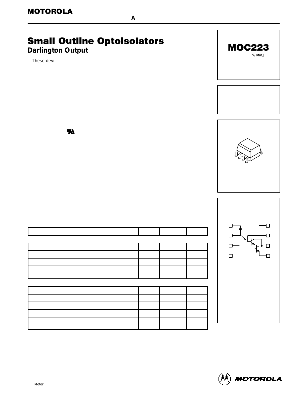
SMALL OUTLINE
OPTOISOLATORS
DARLINGTON OUTPUT
CASE 846–01, STYLE 1
PLASTIC
SCHEMATIC
1. LED ANODE
2. LED CATHODE
3. NO CONNECTION
4. NO CONNECTION
5. EMITTER
6. COLLECTOR
7. BASE
8. NO CONNECTION
1
2
3
8
6
5
4
7
(Replaces MOC221/D)
MOC223
2
Motorola Optoelectronics Device Data
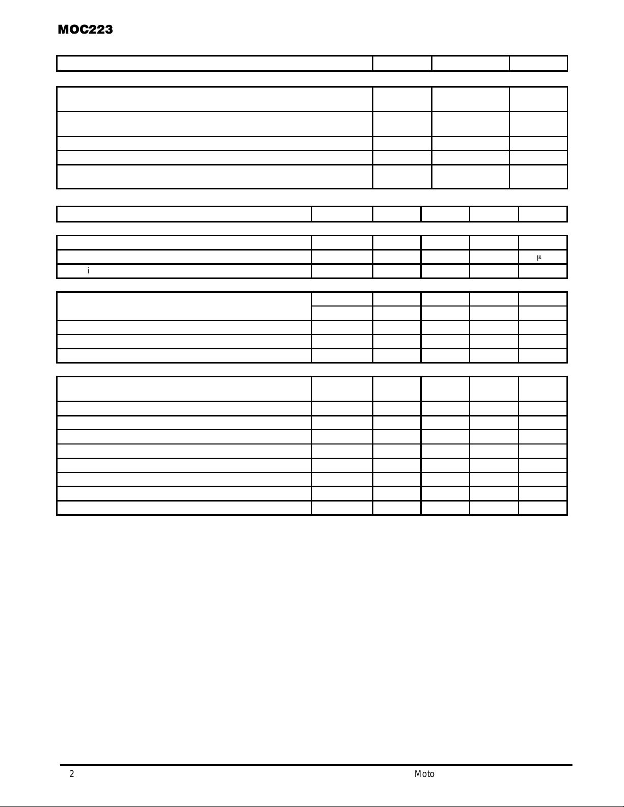
MAXIMUM RATINGS — continued
(TA = 25°C unless otherwise noted)
Rating Symbol Value Unit
TOTAL DEVICE
Input–Output Isolation Voltage
(1,2)
(60 Hz, 1.0 sec. duration)
V
ISO
3000 Vac(rms)
Total Device Power Dissipation @ TA = 25°C
Derate above 25°C
P
D
250
2.94
mW
mW/°C
Ambient Operating Temperature Range
(3)
T
A
–55 to +100 °C
Storage Temperature Range
(3)
T
stg
–55 to +150 °C
Lead Soldering Temperature
(1/16″ from case, 10 sec. duration)
— 260 °C
ELECTRICAL CHARACTERISTICS (T
A
= 25°C unless otherwise noted)
(4)
Characteristic Symbol Min Typ
(4)
Max Unit
INPUT LED
Forward Voltage (IF = 1.0 mA) V
F
— 1.05 1.3 V
Reverse Leakage Current (VR = 6.0 V) I
R
— 0.1 100
m
A
Capacitance C — 18 — pF
OUTPUT DARLINGTON
Collector–Emitter Dark Current (VCE = 5.0 V, TA = 25°C) I
CEO
1 — 1.0 50 nA
(VCE = 5.0 V, TA = 100°C) I
CEO
2 — 1.0 — µA
Collector–Emitter Breakdown Voltage (IC = 100 µA) V
(BR)CEO
30 90 — V
Emitter–Collector Breakdown Voltage (IE = 100 µA) V
(BR)ECO
7.0 7.8 — V
Collector–Emitter Capacitance (f = 1.0 MHz, VCE = 0) C
CE
— 5.5 — pF
COUPLED
Output Collector Current
(IF = 1.0 mA, VCE = 5.0 V)
IC (CTR)
(5)
5.0 (500) 10 (1000) — mA (%)
Collector–Emitter Saturation Voltage (IC = 500 µA, IF = 1.0 mA) V
CE(sat)
— — 1.0 V
Turn–On Time (IF = 5.0 mA, VCC = 10 V, RL = 100 Ω) t
on
— 3.5 — µs
Turn–Off Time (IF = 5.0 mA, VCC = 10 V, RL = 100 Ω) t
off
— 95 — µs
Rise Time (IF = 5.0 mA, VCC = 10 V, RL = 100 Ω) t
r
— 1.0 — µs
Fall Time (IF = 5.0 mA, VCC = 10 V, RL = 100 Ω) t
f
— 2.0 — µs
Input–Output Isolation Voltage (f = 60 Hz, t = 1.0 sec.)
(1,2)
V
ISO
3000 — — Vac(rms)
Isolation Resistance (V
I–O
= 500 V)
(2)
R
ISO
10
11
— — Ω
Isolation Capacitance (V
I–O
= 0, f = 1.0 MHz)
(2)
C
ISO
— 0.2 — pF
1. Input–Output Isolation Voltage, V
ISO
, is an internal device dielectric breakdown rating.
2. For this test, pins 1 and 2 are common, and pins 5, 6 and 7 are common.
3. Refer to Quality and Reliability Section in Opto Data Book for information on test conditions.
4. Always design to the specified minimum/maximum electrical limits (where applicable).
5. Current Transfer Ratio (CTR) = IC/IF x 100%.
 Loading...